Author: zmsh

Industry News

From HBM to Co-Packaged Optics: Why High-Hardness Optical Windows Are Becoming More Important in Next-Generation Semiconductor Equipment

Artificial intelligence is changing semiconductor technology at both ends of the system. Inside the package, chipmakers are increasing computing density through high-bandwidth memory, chiplets, advanced packaging and 3D integration. Outside the package, data centers must move enormous volumes of information between accelerators, switches and memory systems. This is pushing the industry toward faster optical connectivity,

Company News

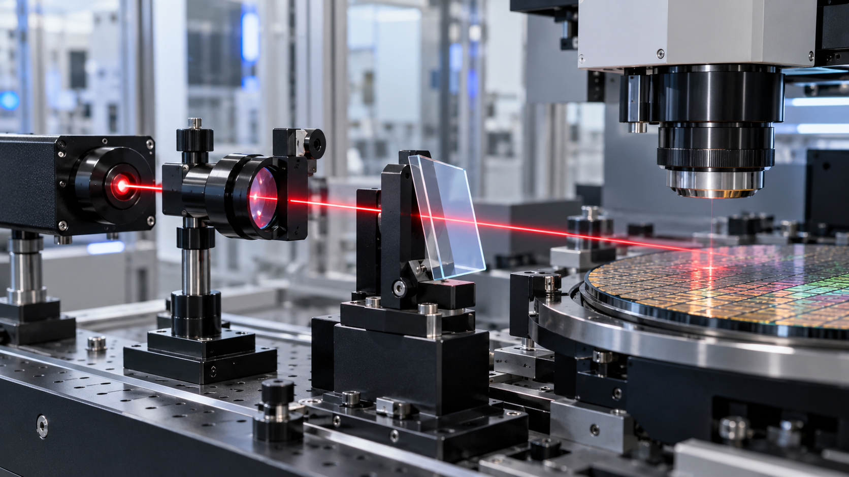
Advanced Semiconductor Inspection Is Entering a New Era: What It Means for Sapphire Windows, Laser Optics and Protective Optical Components

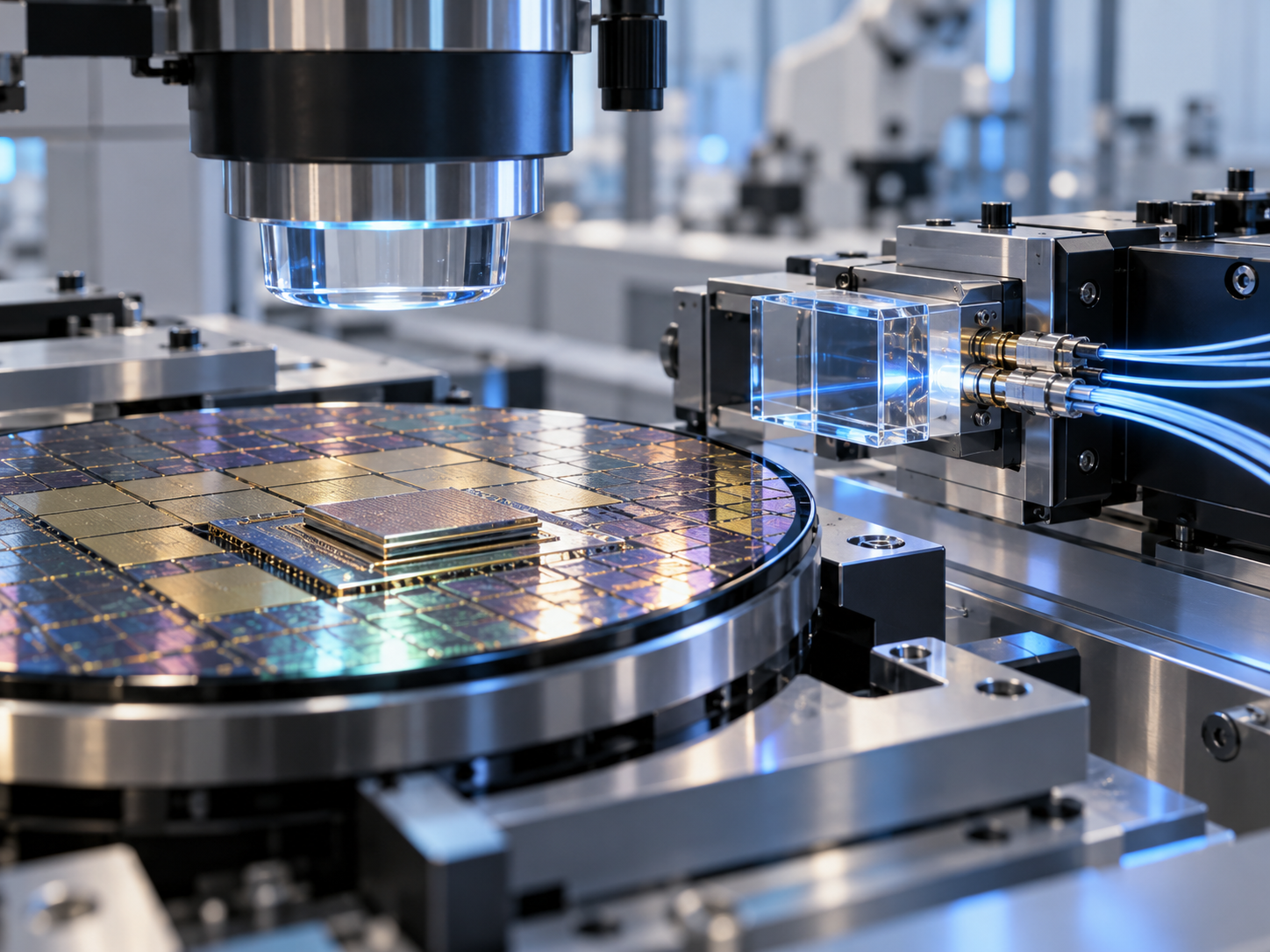
Semiconductor inspection is undergoing a major transformation. For decades, semiconductor metrology was largely associated with measuring wafer dimensions, detecting surface defects and checking individual process layers. Today, the industry must inspect far more complex structures. Chiplets, high-bandwidth memory, 3D stacking, hybrid bonding and advanced packaging are creating devices with features hidden inside multilayer structures rather

Industry News

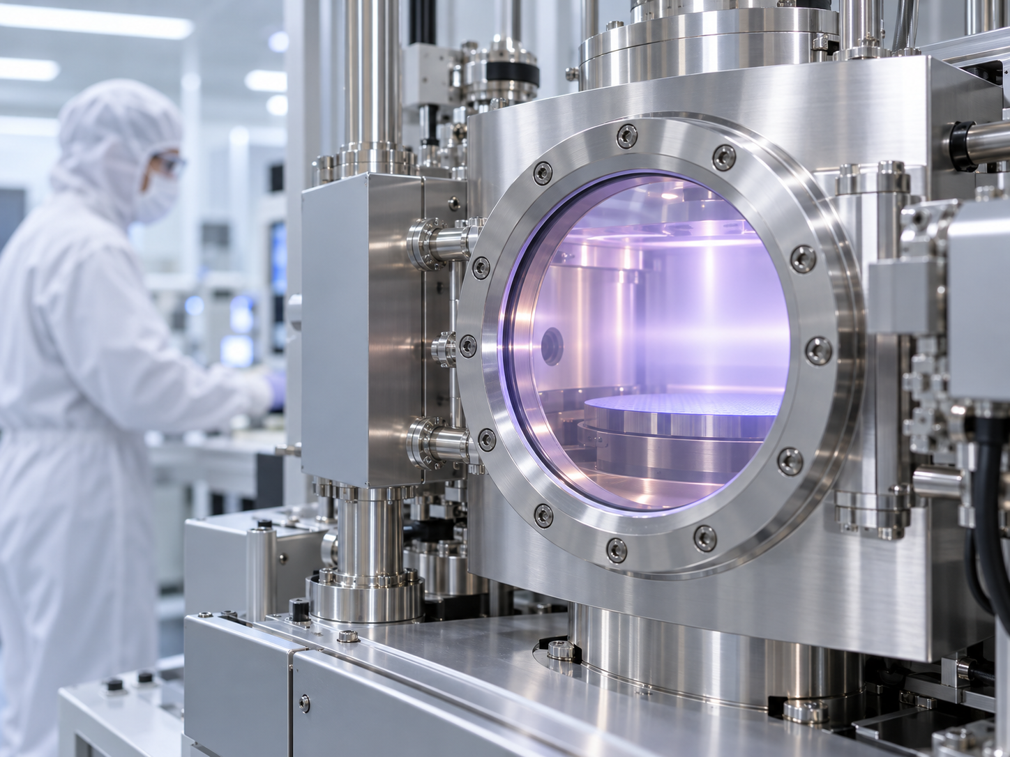
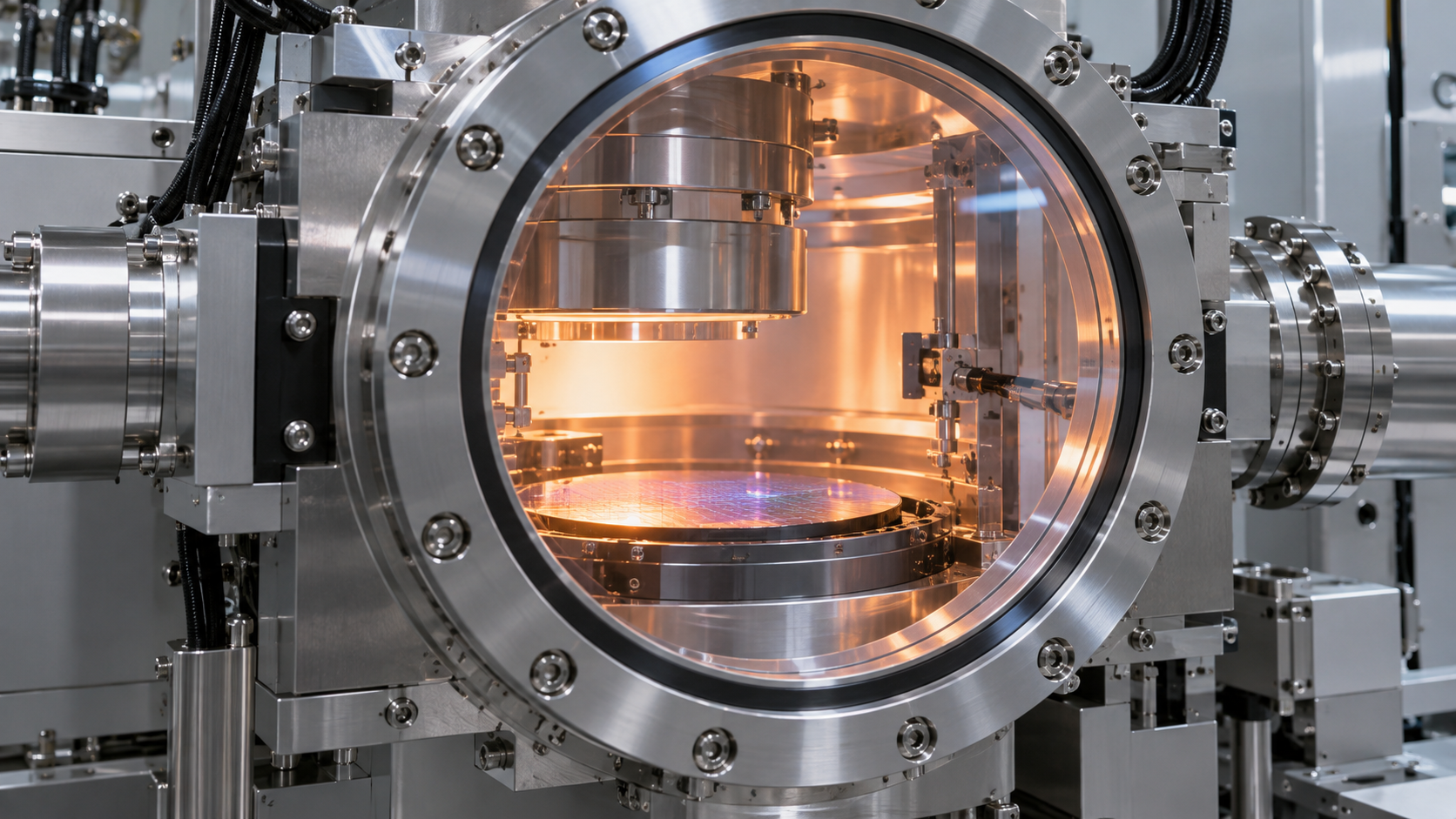
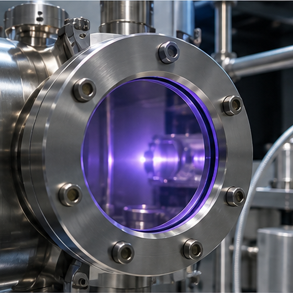
AI Chip Fab Expansion Is Raising Requirements for Semiconductor Optical Windows: Why Sapphire Matters in Plasma, Vacuum and High-Temperature Equipment

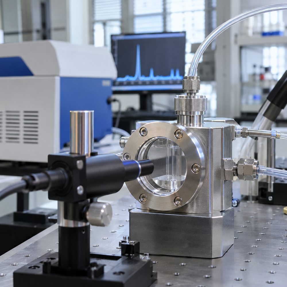
The global semiconductor manufacturing industry is entering another major expansion cycle, driven largely by artificial intelligence, high-performance computing, advanced memory and increasingly complex semiconductor architectures. According to SEMI’s latest 300mm Fab Outlook released in October 2026, global 300mm front-end fab equipment spending is projected to reach approximately US$149 billion in 2026, representing 31% year-over-year growth.

Industry News

Large Sapphire Windows for Advanced Semiconductor Equipment: Thickness Scaling, Flatness, Mounting Stress and Thermal Shock

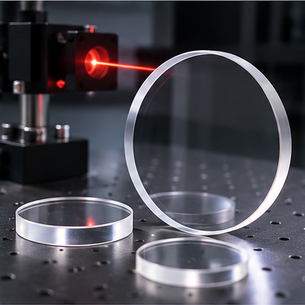
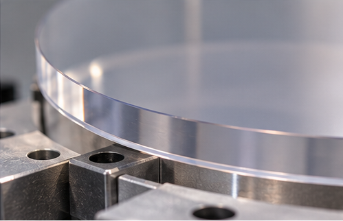
As semiconductor equipment becomes larger, more automated and more optically sophisticated, the size of protective optical windows is also increasing. Large sapphire windows may be used in: At small dimensions, sapphire-window design can appear relatively straightforward. Specify: diameter or length × width × thickness then add the required optical polish. As the window becomes larger,

Company News

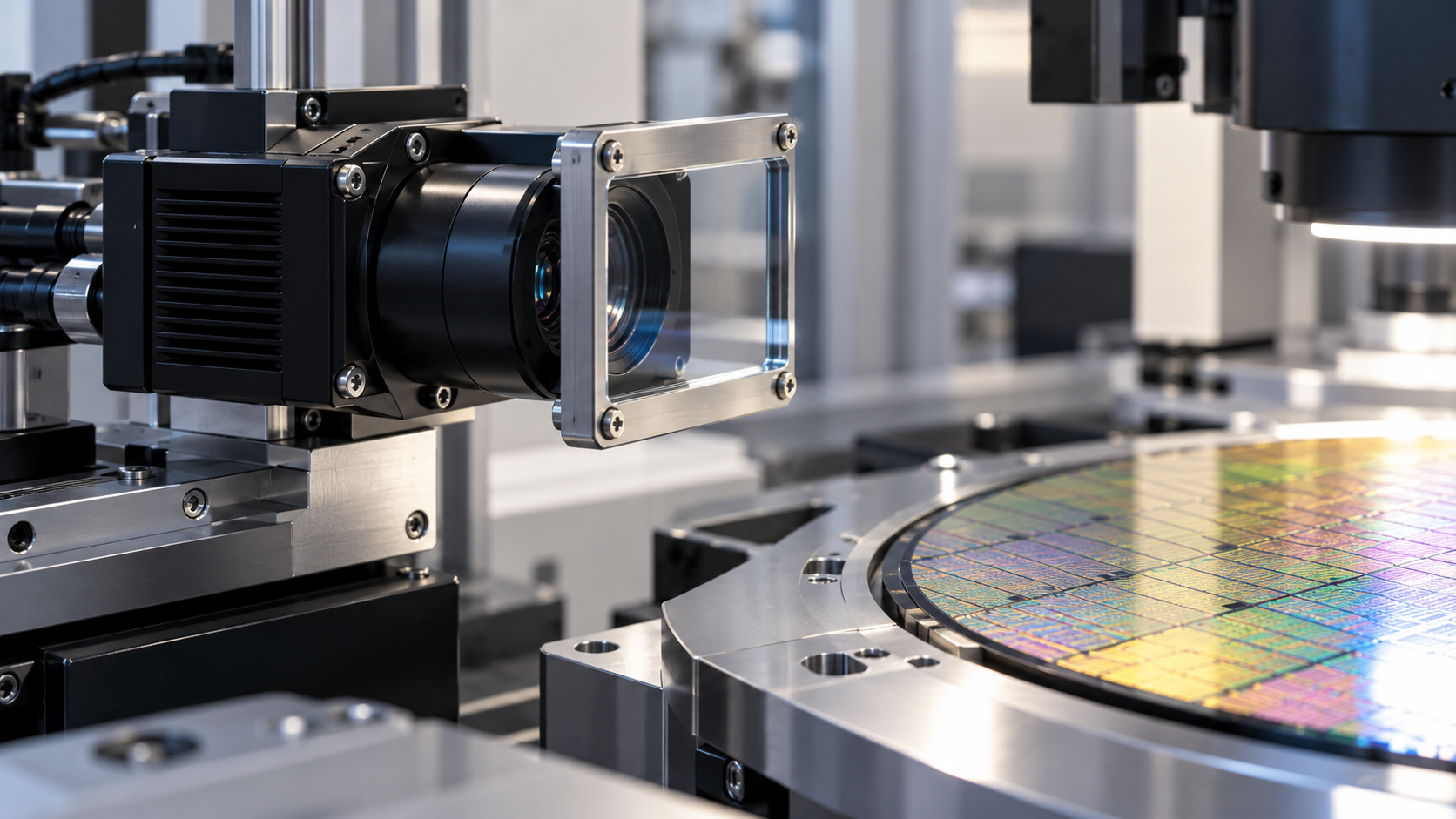
Rectangular Sapphire Windows for Wafer Inspection and Machine Vision: Flatness, Edge Strength, Aspect Ratio and Mounting

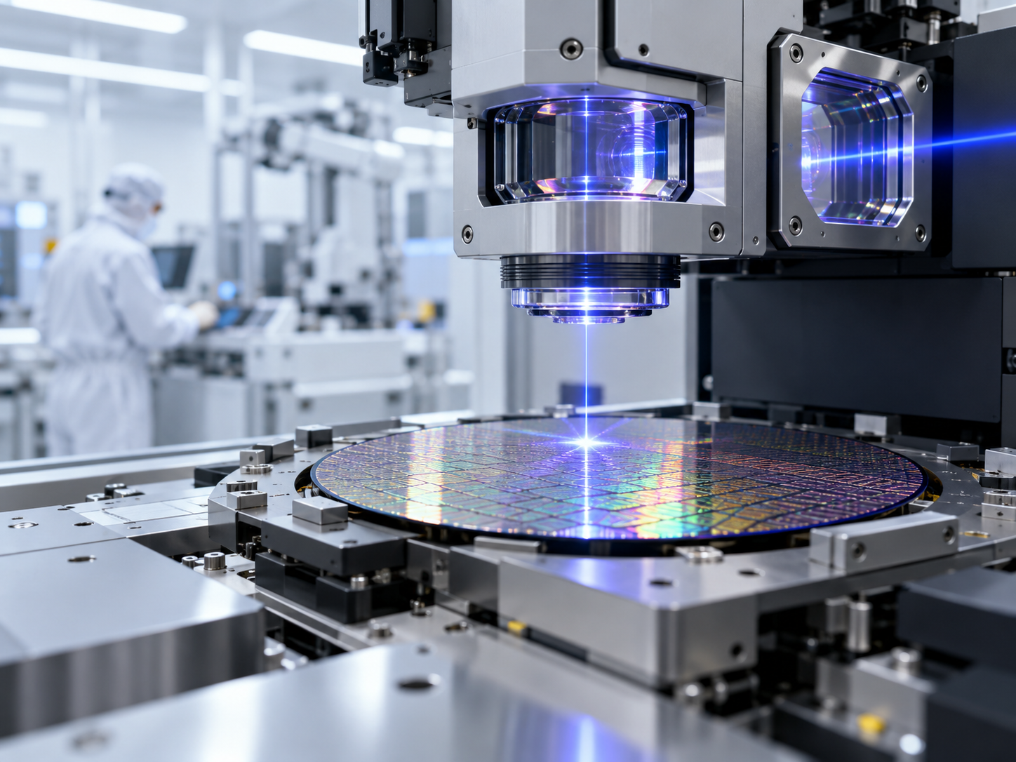
In semiconductor inspection equipment, the optical window is often treated as a passive protective component. In reality, it can directly influence image quality. This becomes especially important in high-resolution wafer inspection, machine vision, laser measurement and automated optical inspection systems. A protective window positioned between the camera or optical sensor and the wafer must transmit