
The global semiconductor manufacturing industry is entering another major expansion cycle, driven largely by artificial intelligence, high-performance computing, advanced memory and increasingly complex semiconductor architectures.
According to SEMI’s latest 300mm Fab Outlook released in October 2026, global 300mm front-end fab equipment spending is projected to reach approximately US$149 billion in 2026, representing 31% year-over-year growth. SEMI also expects investment to continue increasing through 2029, while around 20 new 300mm fabs or production lines are projected to begin construction worldwide in 2026.
Behind these headline numbers lies another important trend: semiconductor manufacturing equipment is being pushed to operate under increasingly demanding plasma, vacuum, thermal and optical environments.
This creates new requirements not only for processing tools but also for the components installed inside them—including optical windows, viewports, protective windows and laser transmission components.
For many of these applications, single-crystal sapphire is becoming an increasingly important engineering material.
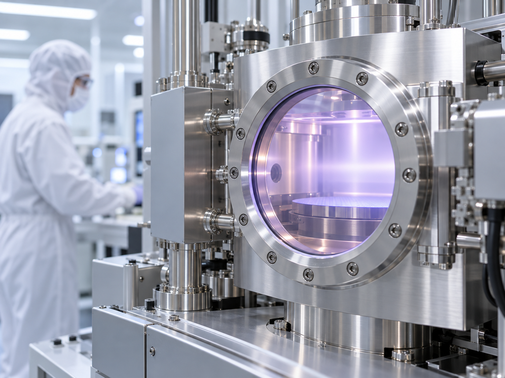
Why Fab Expansion Creates Demand for Specialized Optical Windows
A modern semiconductor fab contains thousands of precision components.
Many process and inspection tools require optical access to a controlled environment. Engineers may need to transmit laser energy into a chamber, observe a process through a viewport, collect optical signals from inside vacuum equipment, or protect sensitive sensors from particles, heat and chemical exposure.
Typical applications can include:
- plasma processing systems;
- vacuum chambers;
- laser processing equipment;
- optical inspection tools;
- wafer alignment systems;
- temperature monitoring equipment;
- deposition and etching systems;
- semiconductor metrology platforms.
A conventional glass window may work well in moderate environments.
However, when a component must withstand a combination of vacuum pressure, elevated temperature, plasma exposure, mechanical contact and repeated cleaning, material selection becomes more critical.
This is where sapphire offers several useful advantages.
Why Sapphire Is Suitable for Harsh Semiconductor Environments
Synthetic sapphire is a single-crystal form of aluminum oxide, Al₂O₃.
Unlike ordinary optical glass, sapphire combines optical transmission with extremely high mechanical hardness.
Its Mohs hardness is approximately 9, second only to diamond among commonly referenced natural materials.
This makes sapphire optical windows highly resistant to scratching and mechanical wear.
For semiconductor equipment, this can be particularly valuable in environments where particles, repeated cleaning cycles or handling can gradually damage softer optical materials.
Sapphire also offers high mechanical strength and good thermal stability.
Depending on the specific design and operating conditions, sapphire components can therefore be considered for applications involving:
- elevated temperatures;
- pressure differentials;
- vacuum environments;
- plasma exposure;
- abrasive particles;
- repeated cleaning;
- mechanically demanding assemblies.
Plasma Processing Places New Demands on Optical Components
Plasma is essential to modern semiconductor manufacturing.
Dry etching, plasma-enhanced chemical vapor deposition and other plasma processes are widely used to create increasingly small and complex semiconductor structures.
Optical windows may be required to provide visual or optical access into plasma chambers.
The challenge is that plasma-processing environments can be highly aggressive.
Depending on the process chemistry, chamber components may encounter energetic ions, reactive gases, elevated temperatures and deposited films.
Any optical component used near such an environment must therefore be selected carefully.
Sapphire’s hardness and chemical durability can make it attractive for selected plasma-facing or plasma-adjacent optical applications.
The exact suitability depends on process gas chemistry, operating temperature, plasma energy, coating requirements and window position.
For this reason, sapphire window specifications should always be matched to the actual semiconductor equipment environment rather than selected only by diameter and thickness.
Vacuum Equipment Requires Mechanical Stability
Vacuum systems are another major application area.
Semiconductor deposition, etching, ion implantation, wafer transfer and analytical systems frequently operate under vacuum.
When an optical window separates atmospheric pressure from a vacuum chamber, it becomes a structural component as well as an optical component.
Important design factors may include:
- window diameter;
- thickness;
- unsupported aperture;
- mounting method;
- sealing structure;
- operating pressure;
- thermal gradients;
- surface quality.
As window diameter increases, mechanical design becomes increasingly important.
Large sapphire windows or sapphire viewports should therefore be engineered according to their actual load conditions rather than using a generic thickness specification.
High Temperature Is Becoming More Important
Advanced semiconductor manufacturing also involves many high-temperature processes.
Furnaces, rapid thermal processing systems, epitaxy tools and specialized research equipment may require optical access for process observation or temperature measurement.
Standard optical glass can encounter limitations when subjected to severe temperature changes or sustained high-temperature environments.
Sapphire has a high melting point and can retain useful mechanical properties at temperatures far above those tolerated by many conventional optical materials.
This makes sapphire windows suitable for consideration in optical monitoring systems exposed to heat.
Thermal shock must still be evaluated carefully.
Material thickness, edge finish, mounting stress and temperature gradient all influence real-world performance.
AI Is Increasing Semiconductor Equipment Complexity
AI demand is not simply creating more fabs. It is also changing the technology installed inside them.
SEMI expects worldwide semiconductor equipment sales to reach approximately US$165.9 billion in 2026, up 23.2% year over year, with growth supported by leading-edge logic, advanced memory, testing and packaging investment.
AI accelerators require increasingly sophisticated manufacturing processes.
HBM requires complex memory fabrication and advanced packaging. Leading-edge logic requires tighter process windows and more precise inspection.
As semiconductor processes become more demanding, equipment manufacturers must increase control over:
- plasma conditions;
- wafer temperature;
- contamination;
- alignment;
- particle levels;
- optical inspection;
- process monitoring.
Optical access becomes part of this control infrastructure.
A small optical window may therefore play a critical role in a multimillion-dollar semiconductor tool.
Surface Quality Matters
Not every sapphire component requires the same optical quality.
For simple visual observation, moderate surface specifications may be acceptable.
Laser transmission and precision imaging applications can require much tighter control.
Common sapphire optical window specifications include:
Surface Quality
Specifications such as 80-50, 60-40, 40-20 or tighter scratch-dig levels may be used depending on optical requirements.
Surface Flatness
Flatness becomes important when the window is part of an imaging or laser path.
Parallelism
Poor parallelism can introduce beam deviation or alignment errors.
Surface Roughness
Precision-polished optical surfaces may require very low roughness.
Edge Quality
Proper chamfering or edge finishing can reduce the risk of chipping during installation and handling.
These requirements should be selected according to actual system performance rather than automatically specifying the tightest tolerance.
Sapphire Crystal Orientation Can Matter
Sapphire is anisotropic.
Its mechanical and optical properties can vary with crystallographic orientation.
Common sapphire orientations include:
- C-plane;
- A-plane;
- R-plane;
- M-plane;
- random orientation.
For many general protective-window applications, orientation may not dominate the design.
For applications involving polarization, birefringence or specific semiconductor processes, however, orientation can become important.
The customer should therefore specify whether crystallographic orientation is critical.
Anti-Reflection Coatings Can Improve Optical Performance
Uncoated sapphire surfaces produce Fresnel reflections.
For optical systems that require higher transmission at a specific wavelength, anti-reflection coatings may be applied.
AR coating designs can be optimized for:
- UV;
- visible;
- near-infrared;
- specific laser wavelengths;
- broad wavelength bands.
However, a coating changes the durability profile of the finished window.
In harsh semiconductor environments, engineers must balance optical performance with coating resistance to plasma, temperature, cleaning chemicals and mechanical contact.
In some systems, an uncoated sapphire window may provide greater long-term durability.
In others, optimized coatings are essential for optical efficiency.
Custom Shapes Are Becoming More Common
Semiconductor equipment designers do not always use standard circular windows.
Custom sapphire optical components may include:
- circular windows;
- rectangular windows;
- square windows;
- sapphire discs;
- sapphire plates;
- stepped windows;
- drilled windows;
- sapphire tubes;
- sapphire domes;
- custom-shaped protective optics.
Features such as holes, slots, edge steps and precision chamfers may be required for equipment integration.
Producing these components requires more than optical polishing. It also requires precision grinding, CNC machining and careful control of edge chipping.
The Future of Sapphire in Semiconductor Equipment
The semiconductor industry’s current investment cycle is unusually broad.
AI is driving leading-edge logic and HBM demand, while governments and manufacturers are simultaneously expanding regional production capacity.
SEMI expects installed 300mm manufacturing capacity to continue growing through the end of the decade.
As more semiconductor equipment enters production, demand will increase not only for wafers and chips but also for the thousands of precision components that make each manufacturing tool possible.
Sapphire optical windows are one part of that ecosystem.
Their combination of hardness, optical transmission, thermal stability and mechanical strength makes sapphire a useful option for semiconductor environments where ordinary optical materials may not provide sufficient durability.
The key is not simply choosing sapphire.
Successful optical-window design depends on correctly matching material grade, orientation, surface quality, flatness, thickness, coating and mechanical geometry to the actual semiconductor process.
As chip fabs become larger and processes become more complex, these details are likely to matter more than ever.