Author: zmsh

Industry News

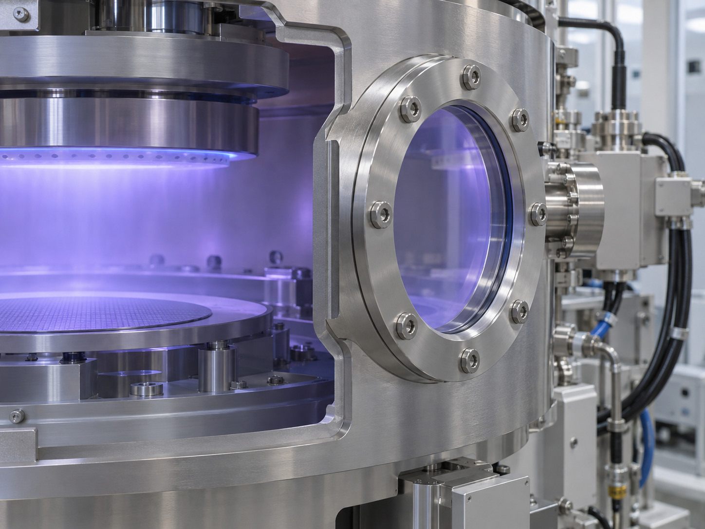
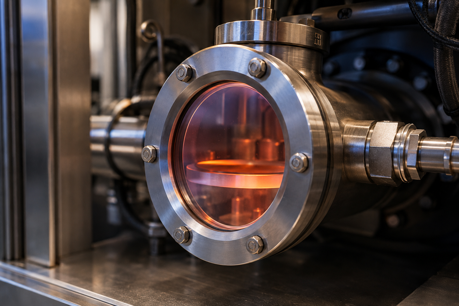
High-Temperature Sapphire Viewports for Vacuum Chambers and Semiconductor Equipment: Thermal Shock, Sealing, Thickness and Optical Quality

Sapphire viewports are increasingly used in vacuum chambers, plasma equipment, semiconductor process tools, high-temperature furnaces and analytical systems where an ordinary glass window may not provide sufficient mechanical, thermal or chemical durability. A sapphire viewport can combine: However, designing a reliable sapphire viewport requires more than selecting a sapphire disc with the correct diameter. The
Industry News

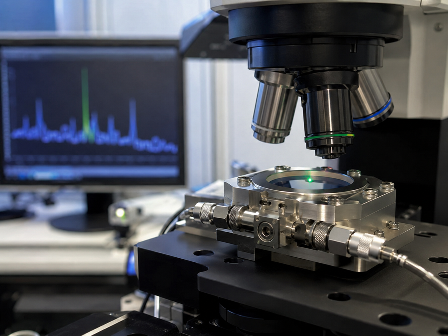
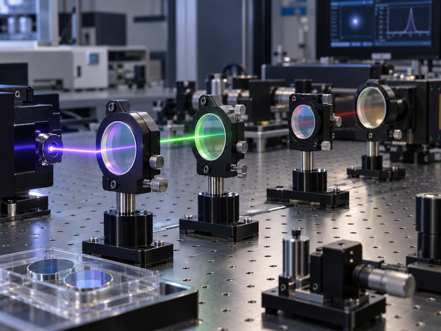
Sapphire Window Coating Selection Guide for 355 nm, 532 nm, 1064 nm and 1550 nm Lasers: AR Bandwidth, AOI, LIDT and Durability

A sapphire window may have excellent mechanical strength, high hardness and good optical transmission, but in a laser system the substrate alone does not determine performance. For many applications, the anti-reflection coating becomes one of the most critical parts of the optical design. A coating specified incorrectly can result in: This becomes especially important at

Industry News

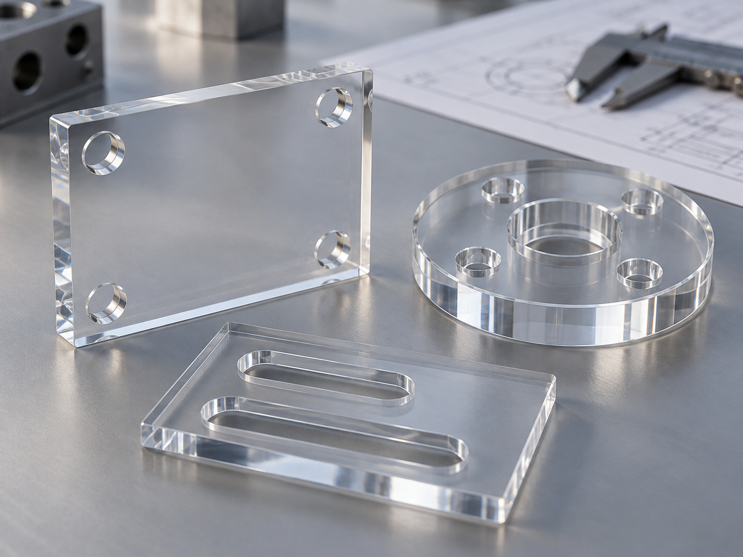
Custom Sapphire Windows with Holes, Slots and Counterbores: CNC Tolerances, Edge Chipping, Stress Concentration and Drawing Guidelines

Standard round or rectangular sapphire windows are relatively straightforward to manufacture. The difficulty increases significantly when a design includes through holes, elongated slots, counterbores, stepped features, internal radii or other machined structures. These features are increasingly common in semiconductor equipment, optical instruments, vacuum systems, laser modules, sensors and precision mechanical assemblies. A custom sapphire component

Industry News

Sapphire Windows for Plasma Etch and PECVD Chambers: Plasma Resistance, Particle Control, Surface Finish and Cleaning Cycles

In plasma etching, PECVD, ICP, RIE and other semiconductor processes, an optical window is rarely just a transparent cover. Depending on its location inside the equipment, the window may be exposed to reactive gases, energetic ions, elevated temperatures, deposition films, repeated chamber cleaning and mechanical stress. At the same time, it may need to maintain

Industry News

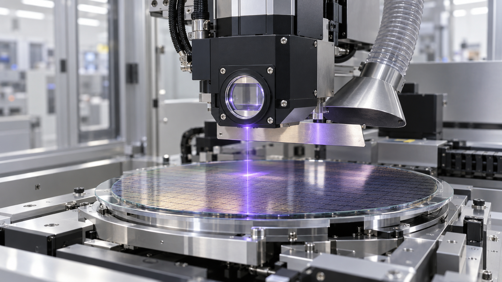
Sapphire Protective Windows for UV Laser Debonding in HBM and Hybrid Bonding: 355 nm Transmission, Laser Damage Threshold, AR Coating and Debris Control

High-bandwidth memory, 3D DRAM and hybrid-bonded semiconductor packages require increasingly thin device wafers and dies. Temporary bonding provides mechanical support while these fragile wafers undergo back grinding, TSV processing, metallization, cleaning, inspection and other manufacturing steps. After processing, the device wafer or functional layer must be separated from its temporary carrier without introducing cracks, excessive

Industry News

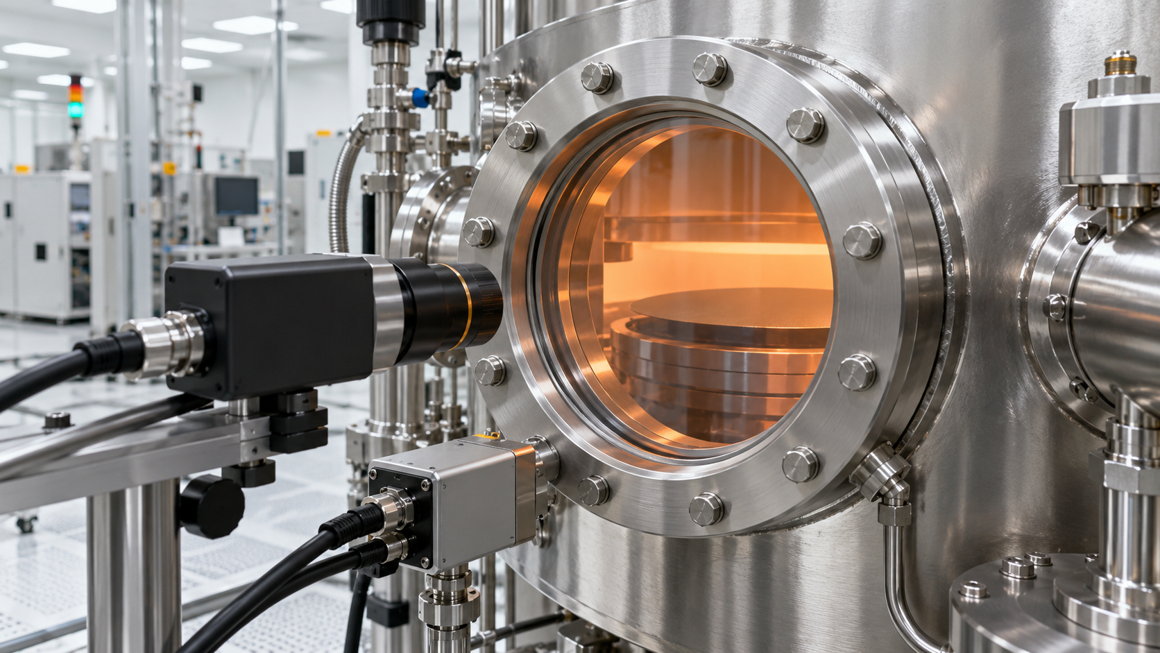
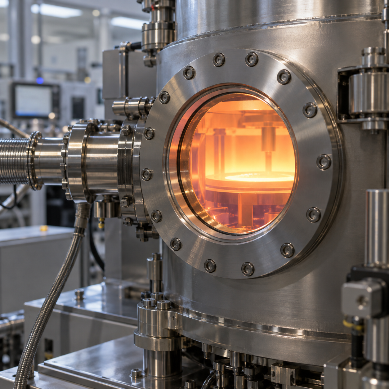
Sapphire Viewports for 200 mm and Future 300 mm SiC Epitaxy Reactors: Pyrometry Wavelengths, Thermal Stress, Deposit Buildup and In-Situ Monitoring

Silicon carbide manufacturing is moving from 150 mm wafers toward 200 mm production. Commercial 200 mm SiC epitaxy platforms are already available, including batch systems capable of processing multiple 200 mm wafers. At the same time, the successful demonstration of a single-crystal 300 mm SiC wafer in 2026 has opened discussion about how future crystal

Industry News

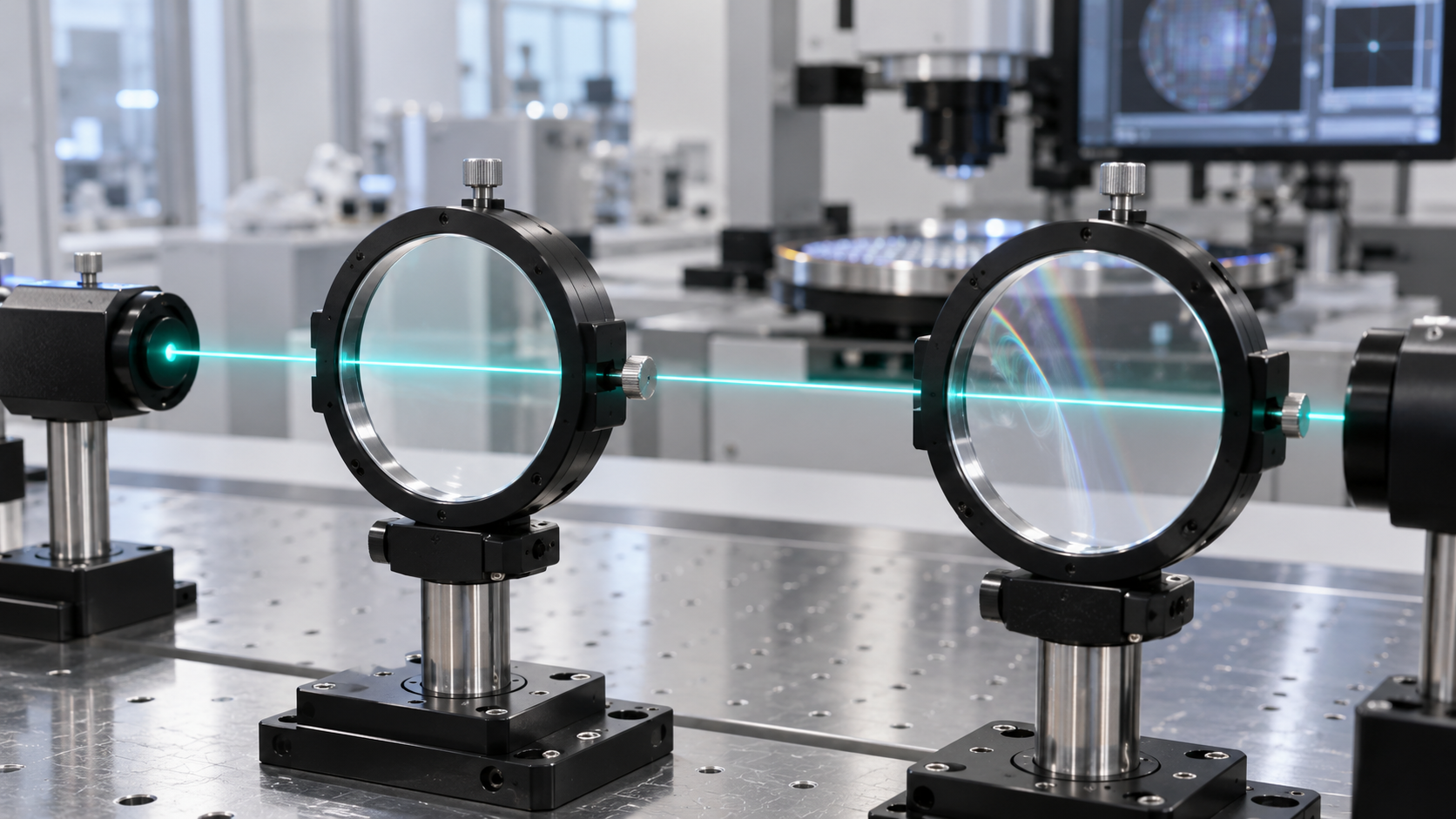
R-Plane vs C-Plane Sapphire Windows for Semiconductor Alignment and Metrology: Birefringence, Polarization, Wavefront Error and Orientation Selection

Sapphire windows are widely used in semiconductor equipment because they combine high hardness, thermal stability, chemical resistance and transmission from the ultraviolet into the mid-infrared region. However, specifying “optical sapphire” is not enough for an alignment, inspection or metrology system. Sapphire is an anisotropic single crystal, which means its optical behavior depends on crystal orientation,

Industry News

Sapphire Windows Under Repeated Thermal Cycling: Thermal Stress, Crack Initiation, Optical Distortion and Service Life

Sapphire windows are widely used in optical systems that must operate under high temperature, vacuum, pressure, abrasion and chemically aggressive environments. Applications range from semiconductor processing chambers and industrial furnaces to aerospace sensors, combustion monitoring systems and high-temperature observation equipment. One of sapphire’s major advantages is its ability to maintain mechanical and optical performance in

Industry News

Sapphire Windows Under Repeated Thermal Cycling: Thermal Stress, Crack Initiation, Optical Distortion and Service Life

Sapphire windows are widely used in optical systems that must operate under high temperature, vacuum, pressure, abrasion and chemically aggressive environments. Applications range from semiconductor processing chambers and industrial furnaces to aerospace sensors, combustion monitoring systems and high-temperature observation equipment. One of sapphire’s major advantages is its ability to maintain mechanical and optical performance in

Industry News

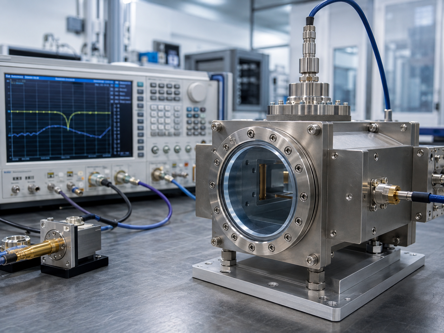
Sapphire Windows for RF and Microwave Systems: Dielectric Constant, Loss Tangent, Frequency, Thickness and Power Handling

Sapphire is widely known as a durable optical window material, but its combination of electrical insulation, low dielectric loss, mechanical strength, thermal stability and vacuum compatibility also makes it useful in selected radio-frequency, microwave and millimeter-wave systems. In these applications, however, a sapphire window cannot be specified only by diameter, thickness and optical surface quality.