
Artificial intelligence is changing semiconductor technology at both ends of the system.
Inside the package, chipmakers are increasing computing density through high-bandwidth memory, chiplets, advanced packaging and 3D integration.
Outside the package, data centers must move enormous volumes of information between accelerators, switches and memory systems.
This is pushing the industry toward faster optical connectivity, including co-packaged optics, or CPO.
The transition is beginning to affect not only chip design but also semiconductor manufacturing, packaging, test and optical-engine production.
In October 2026, NVIDIA announced a major expansion of its semiconductor supply chain. Among the plans, SPIL is targeting a 15-fold increase in optical-engine manufacturing capacity for co-packaged optics by mid-2027, with further expansion planned through 2028. NVIDIA also said advanced packaging and semiconductor test capacity are being expanded to support future AI platforms.
At the same time, SEMI projects worldwide 300mm memory-equipment investment to exceed US$50 billion in 2026, supported largely by AI-driven demand for HBM and advanced memory.
These trends point toward a semiconductor ecosystem where electronics, advanced packaging and photonics are becoming increasingly interconnected.
For manufacturers of optical components, one implication is clear: next-generation semiconductor equipment will require more sophisticated and more durable optical interfaces.
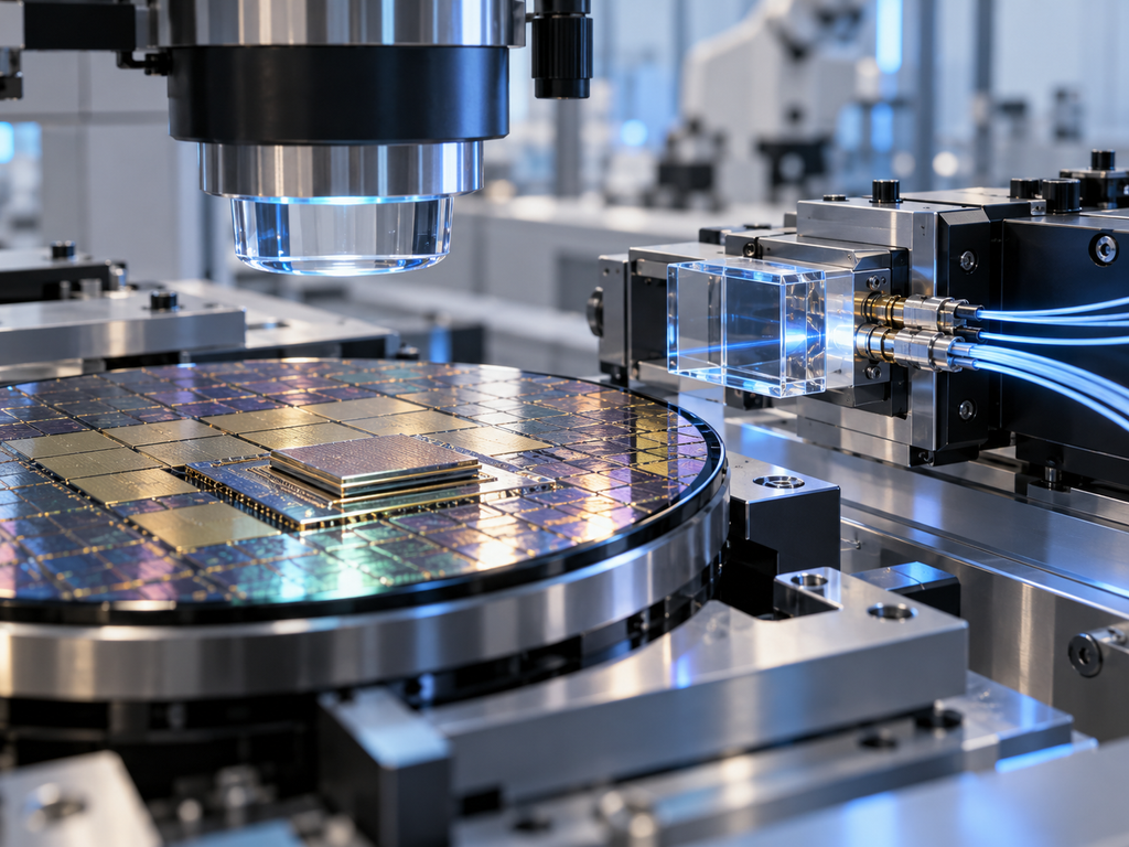
HBM Is Changing Semiconductor Packaging
High-bandwidth memory has become one of the most important technologies supporting AI accelerators.
Rather than placing memory far from the processor, HBM stacks multiple memory dies vertically and positions them close to the computing device.
This increases bandwidth while reducing the distance electrical signals must travel.
Producing HBM requires several demanding manufacturing steps.
These can include:
- wafer thinning;
- through-silicon vias;
- die stacking;
- advanced bonding;
- micro-bump processing;
- wafer inspection;
- packaging inspection.
Every additional process step creates new opportunities for defects.
As a result, manufacturing systems increasingly rely on optical alignment, laser processing and precision inspection.
Why Electrical Interconnects Alone Are Becoming a Limitation
AI systems are growing extremely large.
Thousands of accelerators may need to communicate inside a data-center cluster.
As data rates increase, conventional electrical connections face challenges involving:
- power consumption;
- signal loss;
- heat generation;
- bandwidth density;
- interconnect distance.
Optical communication offers a different approach.
Light can move high-bandwidth data efficiently over distances where electrical connections become increasingly difficult.
Traditionally, optical transceivers have been positioned separately from the main switching chip.
Co-packaged optics aims to move optical engines much closer to the switch ASIC or computing package.
This reduces the distance that high-speed electrical signals need to travel before conversion into optical signals.
CPO Connects Semiconductor Manufacturing With Photonics
Co-packaged optics combines technologies that historically belonged to different manufacturing ecosystems.
A CPO platform may involve:
- advanced CMOS devices;
- silicon photonics;
- optical engines;
- lasers;
- optical fibers;
- precision packaging;
- alignment structures;
- thermal management.
Manufacturing these assemblies requires both semiconductor-scale precision and optical-system accuracy.
That creates new requirements for equipment.
Tools used for optical-engine assembly and testing may need to precisely align optical fibers, photonic dies and laser sources.
Inspection systems may need to evaluate optical coupling while simultaneously checking mechanical placement.
Protective optical windows can be used inside these systems to isolate sensitive optical components from the manufacturing environment.
Why Protective Windows Matter
A laser or camera installed inside semiconductor equipment is expensive and sensitive.
Particles, scratches and contamination on the optical path can affect performance.
A protective window creates a replaceable barrier between the environment and the sensitive optical system.
But the protective window itself must satisfy demanding requirements.
It should provide:
- appropriate optical transmission;
- low surface scattering;
- dimensional stability;
- mechanical durability;
- contamination resistance;
- repeatable optical behavior.
For industrial equipment expected to operate continuously, durability becomes particularly important.
Why Sapphire Is Attractive
Sapphire offers an unusual combination of optical and mechanical properties.
It is transparent over a broad wavelength range and is exceptionally hard.
This high hardness provides strong resistance against scratches and abrasion.
Compared with softer optical materials, sapphire protective windows can better tolerate frequent cleaning and mechanical exposure.
This can be useful in equipment involving:
- automated wafer handling;
- laser processing;
- optical alignment;
- high-speed inspection;
- semiconductor packaging;
- fiber alignment;
- vacuum processing.
However, sapphire is not automatically the best optical material for every CPO application.
Transmission wavelength, birefringence, coating requirements and system design must always be evaluated.
The value of sapphire is greatest where optical performance must be combined with mechanical durability.
Optical Engine Manufacturing Requires Precise Alignment
An optical system is fundamentally different from a purely electrical assembly.
If an electrical contact is slightly displaced but still within its pad area, it may continue to function.
Optical coupling can be much less forgiving.
Small positional errors between:
- lasers;
- waveguides;
- photonic chips;
- lenses;
- fibers
can produce significant optical losses.
This means equipment used to manufacture CPO modules may require highly precise machine vision and optical alignment.
A protective window inside such equipment must avoid introducing unnecessary distortion.
Important parameters can therefore include:
- flatness;
- parallelism;
- transmitted wavefront quality;
- surface roughness;
- scratch-dig;
- AR coating.
HBM and CPO Are Part of the Same AI Infrastructure Trend
HBM and co-packaged optics may appear to be separate semiconductor technologies.
In reality, both are responses to the same underlying challenge: moving more data with less energy.
HBM improves data movement between memory and compute.
CPO aims to improve data movement between chips and systems.
This is why AI investment is simultaneously increasing demand for:
- advanced memory;
- advanced packaging;
- semiconductor test;
- optical connectivity.
SEMI projects 2026 DRAM equipment spending to rise strongly as manufacturers invest in HBM and DDR5 capacity.
NVIDIA’s recently announced supply-chain expansion similarly covers substrates, advanced packaging, semiconductor testing and optical engines rather than treating them as isolated technologies.
The semiconductor production chain is becoming increasingly interconnected.
Laser Processing Will Become More Important
Photonics manufacturing naturally increases the role of lasers.
Lasers may be used for:
- alignment;
- marking;
- measurement;
- fiber coupling;
- dicing;
- trimming;
- inspection;
- active optical testing.
These systems can require protective laser windows.
For laser applications, sapphire-window specifications need to consider more than mechanical strength.
Important variables include:
Laser wavelength
The optical material and coating must provide suitable transmission.
Power density
High optical power can make surface defects and contamination more important.
Pulse duration
Pulsed lasers can produce very high peak power even when average power appears moderate.
Surface quality
Scratches and digs can increase scattering.
Coating quality
AR coatings can reduce reflection but must be designed for the wavelength and operating environment.
Semiconductor Equipment Needs Components That Last
Manufacturing throughput is critical.
A semiconductor production tool that stops operating can affect an entire process flow.
Equipment designers therefore consider not only the initial performance of an optical component but also its lifetime.
A protective window may experience:
- thousands of cleaning cycles;
- mechanical handling;
- vibration;
- temperature changes;
- chemical exposure;
- particles;
- laser radiation.
A softer window material can gradually become scratched.
Sapphire’s hardness can help reduce this form of degradation.
This is especially valuable when the window protects a much more expensive lens, sensor or laser system behind it.
Custom Sapphire Windows for New Equipment Architectures
The rise of advanced semiconductor and photonics equipment is also increasing demand for customized optical geometries.
Not every system can use a standard catalog window.
Equipment manufacturers may require:
- large rectangular sapphire windows;
- thin sapphire plates;
- circular sapphire windows;
- precision holes;
- mounting slots;
- stepped profiles;
- special edge geometries;
- optical coatings.
Producing these parts requires coordination between mechanical machining and optical polishing.
For example, machining a hole into sapphire can create edge chipping if process parameters are not carefully controlled.
Likewise, polishing a large thin sapphire window can be more difficult because flatness and thickness uniformity must be maintained simultaneously.
Large Optical Windows Present Additional Challenges
As semiconductor equipment becomes larger and more complex, optical apertures can also increase in size.
Large sapphire windows introduce engineering challenges involving:
- thickness uniformity;
- flatness;
- residual stress;
- crystal quality;
- polishing uniformity;
- mounting stress.
The larger the clear aperture, the more difficult it becomes to maintain tight optical tolerances.
For this reason, large-window designs should balance performance requirements with manufacturing feasibility.
An unnecessarily tight specification can significantly increase cost without producing measurable improvement in the final equipment.
Choosing the Right Sapphire Window Specification
When designing a sapphire optical component for semiconductor or photonics equipment, buyers should define the operating conditions first.
Useful information includes:
- dimensions;
- clear aperture;
- thickness;
- wavelength range;
- laser wavelength;
- optical power;
- operating temperature;
- vacuum level;
- coating requirement;
- surface quality;
- flatness;
- parallelism;
- crystal orientation;
- edge design.
This allows the manufacturer to determine whether the component should be treated primarily as a mechanical protective window or as a precision optical element.
The distinction can significantly affect manufacturing cost.
From Chips to Optical Systems
The semiconductor industry is moving beyond traditional electrical scaling.
The future AI computing platform will combine several technologies:
advanced logic for computation, HBM for memory bandwidth, advanced packaging for integration and high-speed photonics for communication.
That shift is already becoming visible in capital investment.
SEMI’s 2026 outlook shows strong growth in semiconductor manufacturing equipment driven by advanced logic, memory, packaging and testing.
NVIDIA’s October 2026 supply-chain announcement demonstrates that optical-engine manufacturing for co-packaged optics is also moving toward much larger scale.
The result will be a new generation of semiconductor equipment in which electrical, mechanical and optical technologies increasingly overlap.
Looking Ahead
Sapphire will not become the core material of every co-packaged optics system.
Nor will sapphire replace the silicon photonics devices, optical fibers, lenses or laser sources that perform the primary optical functions.
Its role is different.
Sapphire can provide a durable optical interface where transparency must be combined with hardness, mechanical strength and environmental resistance.
As semiconductor equipment incorporates more lasers, optical inspection, photonic alignment and harsh-environment sensing, the demand for specialized protective optical components is likely to expand.
In the AI era, the semiconductor industry is no longer concerned only with making transistors smaller.
It must also stack chips, move heat, deliver power and transport enormous volumes of data.
From HBM to co-packaged optics, those challenges are creating a new generation of manufacturing technologies—and new requirements for the optical windows that protect and support them.