
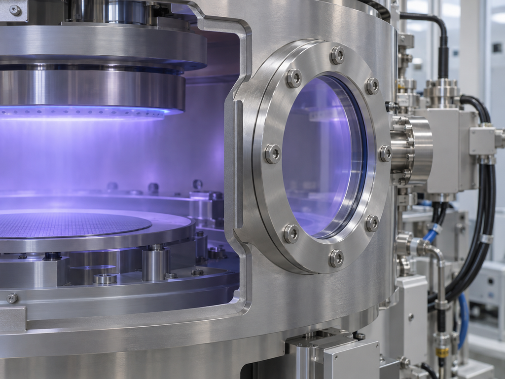
In plasma etching, PECVD, ICP, RIE and other semiconductor processes, an optical window is rarely just a transparent cover.
Depending on its location inside the equipment, the window may be exposed to reactive gases, energetic ions, elevated temperatures, deposition films, repeated chamber cleaning and mechanical stress. At the same time, it may need to maintain stable optical transmission for endpoint detection, pyrometry, optical emission monitoring or process observation.
This combination makes window material selection much more demanding than simply choosing a material with high optical transmission.
Single-crystal sapphire is increasingly considered for demanding semiconductor chamber windows because it combines high hardness, good thermal stability, broad optical transmission and chemical durability. However, sapphire is not universally resistant to every plasma chemistry, and successful use depends heavily on plasma conditions, surface finish, geometry, mounting design and cleaning strategy.
For equipment designers and semiconductor process engineers, the important question is therefore not simply:
“Is sapphire plasma resistant?”
The more useful question is:
“Under my specific plasma chemistry and cleaning cycle, how should the sapphire window be designed and specified to control erosion, particles and optical degradation?”
Why Chamber Windows Are Critical Components in Plasma Equipment
Plasma processing equipment often contains windows or viewports for several different functions.
Typical applications include:
- Optical emission spectroscopy
- Plasma endpoint detection
- Laser-based process monitoring
- Pyrometry
- UV or visible observation
- Infrared temperature measurement
- Laser alignment
- Chamber inspection
- Optical sensor protection
- RF or microwave-related structures in certain equipment designs
These windows may be positioned outside the main plasma region, close to the chamber wall or directly exposed to reactive species.
Their operating environment can include gases such as:
- CF₄
- CHF₃
- C₂F₆
- NF₃
- SF₆
- Cl₂
- BCl₃
- HBr
- O₂
- Ar
In PECVD systems, NF₃-based chamber cleaning is particularly important because deposited films must periodically be removed from chamber surfaces.
As device structures become more complex and contamination requirements become stricter, erosion of chamber-facing materials can become a source of both maintenance problems and process contamination.
A window therefore has to be evaluated as part of the chamber materials system—not as an isolated optical component.
Why Sapphire Is Considered for Plasma Chamber Windows
Sapphire is single-crystal aluminum oxide, Al₂O₃.
Unlike ordinary glass, it combines optical transparency with ceramic-like mechanical properties. Typical sapphire has Mohs hardness around 9 and can transmit from the ultraviolet through visible wavelengths into the mid-infrared, depending on thickness, surface condition and coating.
This combination makes sapphire attractive where a window must simultaneously resist:
- Mechanical scratching
- Repeated cleaning
- Elevated temperature
- Thermal cycling
- Vacuum conditions
- Chemical exposure
- Abrasive deposits
- Optical degradation
Its high hardness is particularly valuable for components that undergo repeated maintenance.
A softer window material may remain optically acceptable when new but gradually accumulate scratches or polishing damage after repeated cleaning. Sapphire provides a much more durable optical surface in this respect.
However, mechanical hardness and plasma resistance are not the same thing.
That distinction is critical when specifying sapphire for semiconductor equipment.
Plasma Resistance: Sapphire Is Durable, but Not Plasma-Proof
One of the most common misconceptions is that sapphire is essentially unaffected by fluorine-based plasma.
That is not correct.
High-density fluorine plasma can react with or physically sputter aluminum-oxide-based materials. Sapphire itself can also be deliberately etched using fluorine-containing plasma under sufficiently energetic ICP-RIE conditions.
The actual erosion rate depends on several interacting parameters:
- Plasma chemistry
- Radical concentration
- Ion energy
- RF power
- Bias power
- Chamber pressure
- Substrate or chamber temperature
- Distance from the plasma
- Angle of exposure
- Duration of each process
- Cleaning frequency
For this reason, two pieces of equipment using the same NF₃ gas can produce very different window lifetimes.
A sapphire window located behind a shield and exposed primarily to reactive radicals may behave very differently from a sapphire component positioned directly inside a high-density plasma region.
Fluorine Plasma
Fluorine-containing chemistries are widely used for semiconductor etching and chamber cleaning.
Under aggressive conditions, long-term fluorine exposure can gradually change the sapphire surface.
Possible effects include:
- Surface roughening
- Microscopic erosion
- Formation of reaction products
- Reduced optical transmission
- Increased scattering
- Particle formation
- Changes in coating condition
This does not mean sapphire is unsuitable.
It means the window should be selected based on the actual plasma exposure rather than on a generic statement such as “excellent chemical resistance.”
Chlorine Plasma
Chlorine-based plasma also requires application-specific evaluation.
Depending on temperature, plasma density and location, sapphire may offer useful durability, but exposed surfaces should still be inspected for roughening, deposits and local erosion.
For high-value semiconductor equipment, qualification testing under the actual chamber chemistry is preferable to relying only on room-temperature chemical compatibility data.
Particle Control May Be More Important Than Optical Transmission
For many semiconductor processes, the biggest risk is not catastrophic window failure.
It is particle generation.
Modern plasma processing places extremely strict demands on chamber cleanliness. As chamber-facing materials gradually erode, microscopic changes can occur on the surface.
These changes may create:
- Loose reaction layers
- Flaking deposits
- Microparticles
- Surface debris
- Contamination from cleaning damage
Particles generated from chamber components can eventually reach the wafer and contribute to yield loss.
Research on plasma-resistant chamber materials increasingly treats erosion rate, surface morphology stability and particle generation as interconnected performance metrics rather than independent material properties.
This is especially important in high-density plasma systems and advanced semiconductor manufacturing, where even small contamination sources become significant.
For a sapphire window, engineers should therefore monitor not only transmission loss but also changes in surface morphology.
A window may still look transparent to the naked eye while its plasma-facing surface has already become significantly rougher.
Why Surface Finish Matters
Surface finish is often specified only as an optical requirement.
In plasma equipment, it can also affect contamination and maintenance behavior.
A high-quality polished sapphire surface provides fewer microscopic irregularities where deposits can mechanically anchor.
Important parameters may include:
- Surface roughness
- Scratch-dig
- Flatness
- Parallelism
- Edge quality
- Bevel quality
- Subsurface damage
For precision semiconductor applications, Ra values in the sub-nanometer range can be achievable with advanced polishing, although the required specification should depend on the application rather than automatically choosing the lowest possible number.
Surface Roughness
A smoother starting surface can provide several advantages:
- Lower optical scattering
- More stable transmission
- Easier inspection
- Reduced sites for deposit adhesion
- Better repeatability after cleaning
However, Ra alone does not describe the complete condition of the surface.
Two windows with similar measured Ra can have different levels of subsurface polishing damage.
This becomes particularly important after repeated plasma exposure and cleaning cycles.
Scratch-Dig
Scratch-dig requirements should be selected according to the optical system.
A chamber observation window may not require the same cosmetic specification as a laser transmission window.
Over-specifying scratch-dig can increase manufacturing cost without improving process performance.
On the other hand, windows used for laser monitoring, spectroscopy or precision imaging may require much tighter surface-quality specifications.
Deposits Can Degrade a Window Before the Sapphire Itself Fails
In PECVD and other deposition processes, window degradation is often caused by deposited film rather than direct attack on the sapphire substrate.
Silicon-containing, nitride, oxide or other films may gradually accumulate on the chamber-facing surface.
This can cause:
- Transmission loss
- Increased optical scattering
- Wavelength-dependent measurement errors
- Reduced signal-to-noise ratio
- Incorrect pyrometry readings
- Endpoint detection instability
For an optical monitoring system, even a modest transmission change can affect measurement repeatability.
Therefore, maintenance intervals should not be determined only by structural window lifetime.
The relevant limit may instead be the point at which optical transmission has shifted beyond the allowable process-control tolerance.
Sapphire Windows for Plasma Endpoint Detection
Optical emission spectroscopy is frequently used to monitor plasma processes.
The detector observes selected emission wavelengths through an optical viewport.
In this application, window performance depends on more than basic transparency.
Engineers should consider:
- Monitoring wavelength
- Sapphire transmission at that wavelength
- Window thickness
- Crystal orientation
- Surface quality
- AR coating
- Angle of incidence
- Plasma deposits
- Temperature
- Expected cleaning cycle
If the system operates at a narrow wavelength, an anti-reflection coating can significantly improve optical throughput.
However, placing a coating directly on a plasma-facing surface can create another failure mechanism.
For aggressive environments, it may be preferable to place the coated surface away from direct plasma exposure whenever the mechanical design allows.
AR Coatings and Plasma Exposure
Bare sapphire has a relatively high refractive index, so reflection losses can be significant when high optical throughput is required.
AR coatings can therefore be useful for:
- UV monitoring
- Visible spectroscopy
- Near-infrared sensors
- Laser alignment
- Pyrometry
But the coating must be considered separately from the sapphire substrate.
A sapphire substrate may survive an environment that gradually damages the coating.
Important coating questions include:
- Which surface will face the chamber?
- Will that surface see direct plasma?
- Which gases are used?
- What temperature will the coating experience?
- How is the window cleaned?
- Is narrowband or broadband AR required?
- What angle of incidence is expected?
For severe plasma exposure, a bare plasma-facing sapphire surface combined with an AR coating on the protected side may be a more robust configuration.
The exact solution depends on the optical system.
Cleaning Cycles Can Determine Real Service Life
A semiconductor chamber window may experience hundreds or thousands of process and cleaning cycles.
Window durability should therefore be considered as a lifecycle problem.
The component experiences repeating stages:
Process → Deposition → Plasma Cleaning → Inspection → Process
Each cycle can slightly change the surface.
Over time, this may produce:
- Roughness growth
- Surface haze
- Reduced transmission
- Coating degradation
- Edge damage
- Deposit accumulation
- Localized erosion
For this reason, specifying a sapphire window only by dimensions and initial transmission is insufficient.
NF₃ Chamber Cleaning
NF₃ is widely associated with cleaning deposited material from PECVD and related chambers.
However, cleaning conditions can also expose chamber materials to reactive fluorine species.
Longer cleaning time is not automatically better.
An unnecessarily aggressive clean may remove chamber deposits but also accelerate wear of chamber-facing components.
Equipment engineers should therefore optimize:
- NF₃ concentration
- Plasma power
- Cleaning duration
- Cleaning frequency
- Chamber temperature
The goal is to remove process deposits without unnecessarily increasing material erosion.
Mechanical Cleaning
Manual maintenance can also damage optical windows.
Metal scrapers, inappropriate abrasive pads or uncontrolled polishing can introduce scratches even on a hard sapphire surface.
Recommended maintenance procedures should clearly define:
- Approved cleaning chemistry
- Approved wipes
- Particle removal method
- Maximum mechanical force
- Inspection method
- Reuse criteria
Sapphire’s hardness provides a strong advantage, but poor cleaning practices can still damage edges, coatings or polished surfaces.
When Should a Sapphire Chamber Window Be Replaced?
Replacement should ideally be based on measurable criteria rather than appearance alone.
Possible replacement criteria include:
1. Transmission Loss
Measure transmission at the actual operating wavelength.
A broadband visible inspection may not reveal degradation that matters at a specific UV or IR wavelength.
2. Surface Roughness Increase
Compare the used surface with the original specification.
A significant increase may indicate plasma erosion.
3. Haze or Scattering
Haze can affect optical monitoring even when total transmission remains relatively high.
4. Particle Generation
Any evidence that the window surface is becoming a contamination source should trigger investigation.
5. Coating Damage
Peeling, cracking or localized coating failure may change optical performance or create particles.
6. Edge Damage
Small edge chips should not automatically be ignored.
Under vacuum loading or thermal cycling, damaged edges may become stress concentration points.
Important Specifications for Custom Sapphire Chamber Windows
When requesting a custom sapphire window for plasma etch or PECVD equipment, the following information helps the manufacturer evaluate feasibility.
| Parameter | Typical Information Required |
|---|---|
| Window shape | Round, square, rectangular, ring or custom |
| Diameter / dimensions | According to equipment drawing |
| Thickness | Based on mechanical and optical requirements |
| Crystal orientation | C-plane, A-plane, R-plane or application-specific |
| Surface roughness | According to optical/process requirement |
| Surface quality | Scratch-dig specification |
| Flatness | Depending on imaging or sealing requirement |
| Parallelism / wedge | Important for beam deviation |
| Edge | Chamfer, bevel or radius |
| Clear aperture | Optical usable area |
| Coating | Uncoated or AR coated |
| Wavelength | UV, VIS, NIR or IR |
| Plasma chemistry | NF₃, CF₄, SF₆, Cl₂, BCl₃, etc. |
| Process temperature | Maximum operating temperature |
| Chamber pressure | Vacuum/process condition |
| Cleaning process | Plasma clean and/or wet clean |
| Mounting method | O-ring, metal seal, clamp or bonded assembly |
Providing these parameters early can reduce unnecessary iterations between the optical supplier and equipment engineer.
Thickness Should Not Be Selected by Diameter Alone
A common RFQ may specify something like:
100 mm diameter × 2 mm sapphire window
without explaining the pressure or mounting conditions.
This is not enough for structural evaluation.
Required thickness depends on:
- Unsupported diameter
- Pressure differential
- Mounting geometry
- Edge support
- Operating temperature
- Thermal gradient
- Safety factor
- Crystal orientation
Vacuum windows may experience approximately one atmosphere of external differential pressure during operation.
Large-diameter thin windows therefore require proper mechanical analysis.
Increasing thickness improves structural safety but can affect cost, absorption, optical path length and system geometry.
The optimum design is a balance between optical and mechanical requirements.
Edge Design Is Often Overlooked
Window failure risk is frequently concentrated at the edge rather than the central polished area.
Sharp edges and machining defects can act as stress concentrators.
For chamber applications, edge specifications should include:
- Chamfer width
- Chamfer angle
- Edge radius
- Maximum allowable chip size
- Mounting contact area
The sealing or clamping system should avoid creating highly localized stress.
This becomes increasingly important for large windows and systems exposed to thermal cycling.
Sapphire vs Quartz for Plasma Chamber Windows
Quartz remains widely used in semiconductor equipment because of its excellent optical properties, high purity and established process compatibility.
Sapphire should not automatically be considered a replacement for quartz.
The choice depends on the process.
Sapphire may be attractive where the design requires:
- Higher mechanical hardness
- Better scratch resistance
- High structural strength
- Repeated cleaning
- High-temperature stability
- Compact window thickness
- Long-term mechanical durability
Quartz may remain preferable in other optical, thermal or plasma conditions.
The correct comparison should therefore be based on the actual chamber environment rather than on one material property.
Questions to Ask Before Ordering
Before manufacturing a custom sapphire chamber window, an equipment engineer should ideally answer the following questions:
- What gases contact the window?
- Is the window directly exposed to plasma?
- What is the RF or plasma power?
- What is the maximum operating temperature?
- Is NF₃ or another fluorine chemistry used for chamber cleaning?
- How often is the chamber cleaned?
- What wavelength passes through the window?
- Is an AR coating required?
- What is the required clear aperture?
- What pressure differential must the window withstand?
- How is the window mounted?
- What level of surface roughness and scratch-dig is actually required?
These details allow the sapphire window to be designed around the process rather than treated as a generic optical component.
Frequently Asked Questions
Is sapphire resistant to NF₃ plasma?
Sapphire offers useful chemical and mechanical durability, but it should not be considered completely immune to NF₃ plasma. Under sufficiently energetic fluorine-plasma conditions, sapphire can be etched or its surface can gradually roughen. Actual lifetime depends on plasma power, ion energy, temperature, exposure location and cleaning duration.
Can sapphire be used in PECVD chambers?
Yes. Sapphire can be considered for optical monitoring windows, protective windows and other suitable components in PECVD equipment, particularly where mechanical hardness, thermal stability and repeated cleaning resistance are important. The final design should be evaluated against the specific deposition and cleaning chemistry.
Can sapphire be used for plasma endpoint detection?
Yes. Sapphire’s broad optical transmission makes it suitable for many UV, visible and near-infrared monitoring systems. The wavelength, thickness, surface finish, crystal orientation and coating should be specified according to the detector.
Does lower surface roughness always mean longer chamber life?
Not necessarily. Low initial roughness is beneficial for optical quality and contamination control, but plasma resistance also depends on chemistry, ion energy, temperature and subsurface material condition.
Should AR coating be applied to the plasma-facing surface?
Not automatically. A coating exposed directly to aggressive plasma may degrade faster than the sapphire substrate. Where possible, engineers may consider placing the AR coating on the protected optical side, depending on system design.
How often should a sapphire window be replaced?
There is no universal number of wafers or cleaning cycles. Replacement should be based on measurable indicators such as transmission loss, surface roughness, haze, coating degradation, edge damage and particle performance.
Conclusion
Sapphire windows can provide a valuable combination of optical transparency, hardness, thermal stability and mechanical durability for plasma etch, PECVD and related semiconductor processing equipment.
However, successful chamber-window design requires more than selecting sapphire as the material.
Plasma chemistry, ion energy, temperature, surface quality, coatings, edge geometry, mounting method and cleaning cycles all influence real service life.
For high-value semiconductor applications, the most reliable approach is to define the sapphire window according to the actual process environment.
When requesting a custom component, provide the equipment drawing together with plasma chemistry, process temperature, operating wavelength, cleaning method and required optical specifications.
This allows the sapphire window to be optimized not only for initial optical performance, but also for long-term particle control, maintenance stability and reliable operation inside the semiconductor process environment.