
Semiconductor inspection is undergoing a major transformation.
For decades, semiconductor metrology was largely associated with measuring wafer dimensions, detecting surface defects and checking individual process layers.
Today, the industry must inspect far more complex structures.
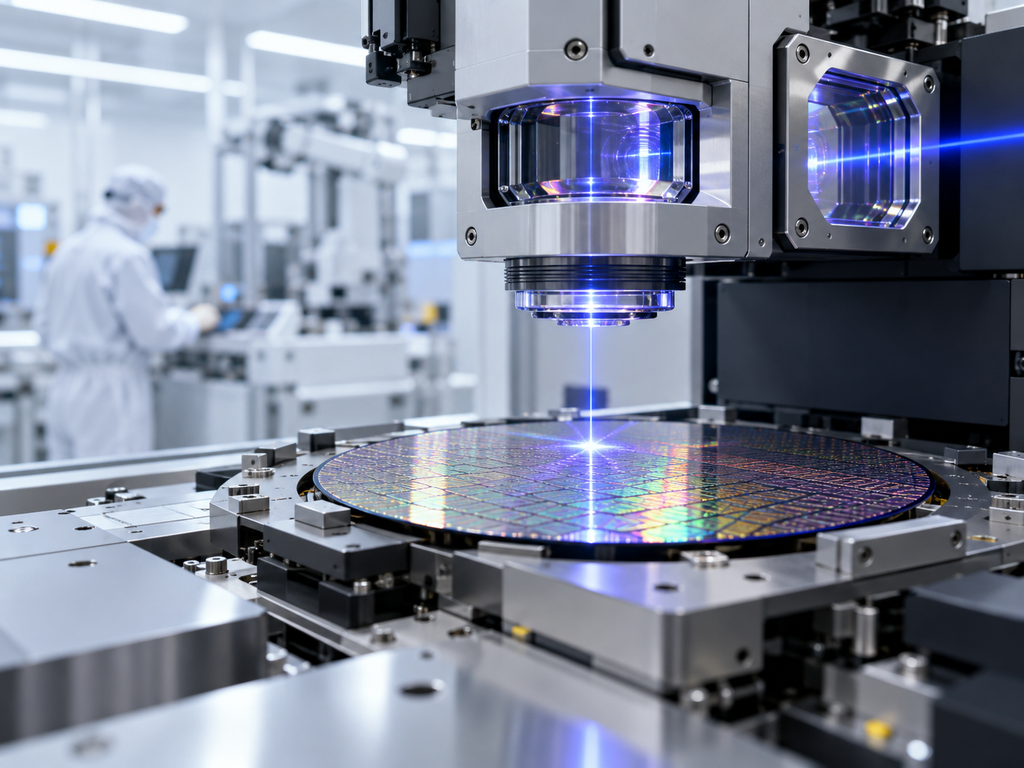
Chiplets, high-bandwidth memory, 3D stacking, hybrid bonding and advanced packaging are creating devices with features hidden inside multilayer structures rather than exposed only at the wafer surface.
This is changing both inspection equipment and the optical components used inside it.
At SEMICON West in October 2026, ZEISS highlighted new inspection and wafer-shape-control technologies for advanced packaging, including inline 3D X-ray inspection and systems designed to measure and correct wafer deformation. ZEISS noted that complex chiplet architectures require manufacturers to inspect internal connections and deformation while maintaining high production throughput.
The development illustrates a broader trend: as semiconductor structures become more complex, inspection systems require increasingly stable, precise and durable optical paths.
For sapphire-window manufacturers, this creates new opportunities in protective optics, laser windows and specialized equipment components.
Why Semiconductor Inspection Is Becoming More Difficult
Traditional semiconductor devices were largely fabricated in two dimensions.
Modern advanced packaging changes this architecture.
Multiple dies may now be stacked vertically or positioned side by side inside a single package.
HBM, for example, integrates multiple memory dies into vertically stacked structures.
Chiplet-based processors can combine logic, memory and specialized computing dies inside one package.
Hybrid bonding can connect these components at extremely fine pitches.
Manufacturers therefore need to inspect:
- wafer surfaces;
- internal package structures;
- bonded interfaces;
- alignment accuracy;
- wafer bow and warp;
- micro-bumps;
- TSV structures;
- cracks;
- voids;
- contamination;
- edge defects.
No single inspection technology can measure everything.
Modern tools may combine visible light, infrared, lasers, X-rays and other sensing techniques.
Optical Windows Are Part of the Measurement System
It is easy to focus on cameras, lasers and sensors when discussing semiconductor inspection.
But every optical system also contains supporting components.
A laser beam may need to pass through a protective window before reaching a wafer.
A camera may observe a process through a chamber viewport.
Sensitive optical components may need protection from particles, cleaning chemicals or mechanical contact.
The window may look simple, but it can influence:
- transmission;
- image quality;
- beam direction;
- reflection;
- distortion;
- system stability.
For high-resolution semiconductor inspection, window quality therefore becomes important.
Why Sapphire Is Used as a Protective Optical Material
Sapphire combines optical transparency with exceptional mechanical hardness.
Its Mohs hardness of approximately 9 makes it far more scratch resistant than most conventional optical glasses.
This characteristic is particularly useful when an optical window is repeatedly cleaned or operates near moving equipment and particles.
Scratches on a protective window can create:
- stray light;
- scattering;
- image artifacts;
- reduced laser transmission;
- false defect signals.
Replacing a damaged optical component inside semiconductor equipment can also mean tool downtime.
A durable sapphire protective window can therefore offer advantages where long-term mechanical resistance is important.
Scratch-Dig Becomes More Than a Cosmetic Specification
Scratch-dig is one of the most common optical surface specifications.
Typical commercial specifications may include:
- 80-50;
- 60-40;
- 40-20;
- 20-10;
- tighter custom specifications.
Lower values generally indicate stricter limits on visible surface imperfections.
For an ordinary mechanical cover, 80-50 may be sufficient.
For precision imaging or laser applications, 40-20 or tighter specifications may be considered.
The correct requirement depends on:
- laser wavelength;
- beam diameter;
- power density;
- imaging resolution;
- focal location;
- optical path sensitivity.
Over-specifying surface quality can unnecessarily increase manufacturing cost.
Under-specifying it may reduce system performance.
For semiconductor inspection windows, the specification should therefore be based on the actual optical function.
Flatness Matters in Precision Imaging
A protective window is not optically neutral simply because it is transparent.
If its surfaces are not sufficiently flat, the window can distort transmitted wavefronts.
This can affect:
- imaging accuracy;
- focusing;
- interferometry;
- beam alignment;
- dimensional measurement.
Surface flatness requirements are commonly expressed relative to an optical wavelength, for example λ, λ/2, λ/4 or tighter.
Not every semiconductor tool requires extremely tight flatness.
But when an optical window sits inside a high-resolution measurement path, flatness may become a critical specification.
Parallelism and Wedge
Parallelism is another important parameter.
If the two surfaces of a window are not parallel, the component behaves like a weak optical prism.
This can shift the transmitted beam.
For simple observation this may be insignificant.
For laser-based wafer alignment or high-precision metrology, even small angular deviation can affect system calibration.
Customers should therefore distinguish between general-purpose protective sapphire windows and precision optical sapphire windows.
The same material can be manufactured to very different optical tolerance levels.
Laser-Based Inspection Creates Additional Requirements
Laser technology is widely used throughout semiconductor manufacturing.
Applications include:
- wafer alignment;
- surface inspection;
- thickness measurement;
- interferometry;
- laser marking;
- laser dicing;
- spectroscopy;
- process monitoring.
Protective optical windows used in these systems must maintain stable transmission.
Important parameters include:
- wavelength;
- laser power;
- pulse duration;
- spot size;
- surface quality;
- coating performance;
- contamination level.
For high-power systems, even small defects or contamination particles can increase localized absorption.
This may lead to heating or optical damage.
Cleaning and packaging therefore become important parts of optical-component quality.
AR Coatings Need to Match the Application
Sapphire has useful optical transmission, but its refractive index produces noticeable surface reflection.
Anti-reflection coatings can increase transmission at the target wavelength.
For semiconductor inspection equipment, coatings may be designed for:
- ultraviolet wavelengths;
- visible wavelengths;
- near-infrared wavelengths;
- specific laser lines;
- broadband inspection systems.
A coating should not be selected solely based on transmission.
Its environmental durability must also be considered.
Cleaning chemicals, thermal cycling and plasma exposure may influence coating lifetime.
For protective optics in harsh environments, the most optically efficient coating is not always the most durable design.
Wafer Warpage Is Becoming a Major Measurement Challenge
Advanced packaging adds another inspection problem: wafers and packages are not perfectly flat.
ZEISS highlighted wafer deformation control as a key challenge in its 2026 advanced packaging portfolio. Its DUNE system is designed to measure wafer topography and support correction of deformation before subsequent processing steps.
As wafers become thinner and contain more layers, differences in thermal expansion can generate significant bow and warp.
This affects:
- bonding;
- lithography;
- handling;
- alignment;
- inspection.
Measurement systems must therefore deliver high precision across large wafer areas.
Optical components inside these systems must maintain stable geometry and optical performance.
Inspection Is Moving Into High-Volume Manufacturing
One important change is that advanced inspection is no longer limited to research laboratories.
ZEISS’s latest systems are aimed at both process development and high-volume manufacturing, including inspection of 300mm wafers.
That changes the reliability requirement.
An optical component used occasionally in an R&D tool may tolerate frequent manual adjustment or replacement.
An optical component used continuously in a production environment must support:
- long operating cycles;
- repeatable calibration;
- low contamination;
- automated equipment;
- minimal maintenance.
Durability becomes just as important as optical performance.
Custom Sapphire Components for Inspection Equipment
Inspection and metrology systems can require many different sapphire geometries.
These may include:
Round Optical Windows
Used for standard beam transmission or chamber observation.
Rectangular Sapphire Windows
Useful in line-scan imaging systems and elongated optical apertures.
Protective Sapphire Covers
Installed directly in front of expensive sensors or camera systems.
Laser Windows
Manufactured with tighter surface quality, flatness and coating specifications.
Sapphire Plates With Holes or Slots
Designed for customized mechanical integration.
Thin Sapphire Discs
Used where low optical path length or compact assemblies are important.
Precision machining allows these components to be integrated directly into equipment designs.
Surface and Edge Inspection Matter Too
The quality of an optical component cannot be judged only by its central surface.
Edges can be equally important.
Poorly processed sapphire edges may contain chips or microcracks that become failure origins during installation or thermal cycling.
Typical edge-processing options include:
- fine grinding;
- chamfering;
- beveling;
- polished edges;
- radius edges.
Inspection should therefore evaluate both optical surfaces and mechanical edges.
The Future of Semiconductor Inspection
SEMI expects semiconductor test-equipment sales alone to grow significantly in 2026 as AI-related investment expands across advanced logic, memory and packaging.
At the same time, advanced packaging is moving inspection requirements deeper inside semiconductor structures.
The industry is shifting from asking simply, “Is there a defect on the wafer surface?” to asking:
Where is the defect?
Is it inside the package?
Is the bond interface complete?
Has the wafer deformed?
Are stacked dies aligned?
Can the defect be detected early enough to protect yield?
Answering these questions requires increasingly sophisticated combinations of optics, lasers, X-rays, sensors and precision mechanics.
Sapphire windows will not replace the complex optical systems that make these measurements possible.
But they can perform an important supporting role by protecting sensitive optical paths while maintaining mechanical and optical stability.
As inspection moves toward higher resolution, greater automation and continuous high-volume production, the quality of even seemingly simple optical components will become increasingly important.
In advanced semiconductor equipment, the protective window is no longer just a piece of transparent material.
It is part of the measurement system.