Company News
Advanced Semiconductor Inspection Is Entering a New Era: What It Means for Sapphire Windows, Laser Optics and Protective Optical Components
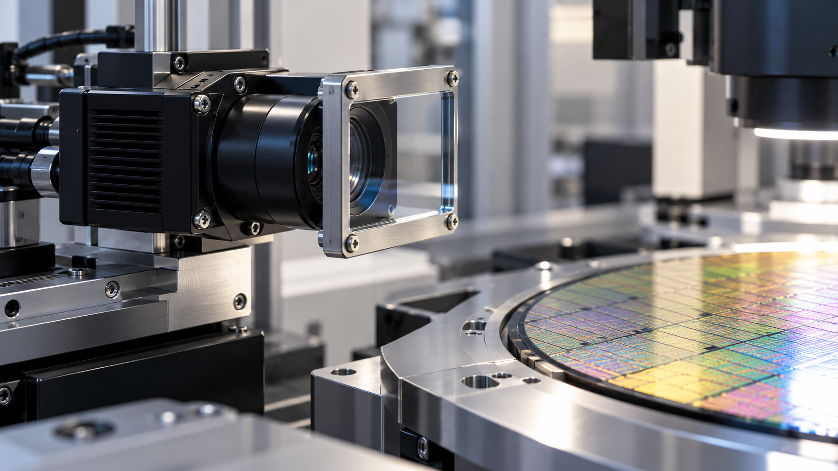
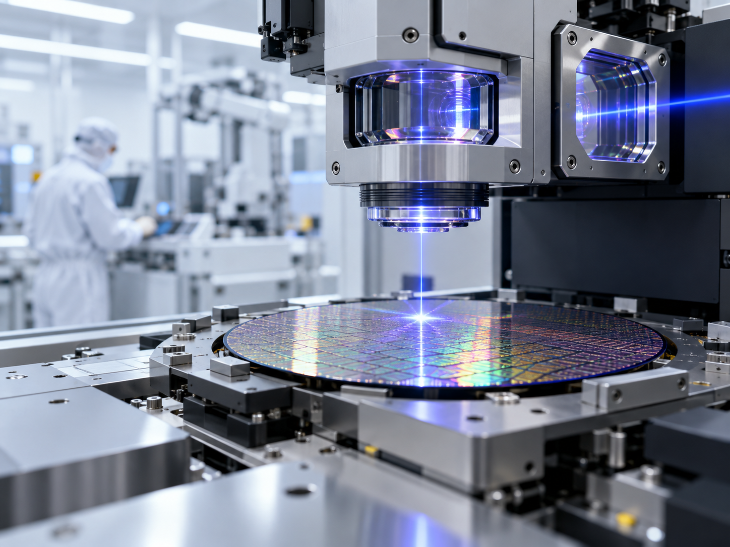
Semiconductor inspection is undergoing a major transformation. For decades, semiconductor metrology was largely associated with measuring wafer dimensions, detecting surface defects and checking individual process layers. Today, the industry must inspect far more complex structures. Chiplets, high-bandwidth memory, 3D stacking, hybrid bonding and advanced packaging are creating devices with features hidden inside multilayer structures rather