
В передовой электронике и оптоэлектронике выбор материала напрямую определяет производительность устройства, его надежность и структуру затрат. Среди наиболее широко обсуждаемых материалов подложек - кремниевые пластины и сапфировые подложки.
Хотя оба материала используются в отраслях, связанных с полупроводниками, их роль принципиально различна. Кремний доминирует в традиционных интегральных схемах, в то время как сапфир все чаще используется в оптоэлектронике, высокочастотных устройствах и приложениях для работы в жестких условиях.
В этой статье приводится более глубокое техническое сравнение с практической инженерной точки зрения с акцентом на электрическое поведение, оптические свойства, тепловые характеристики и реальные примеры использования.
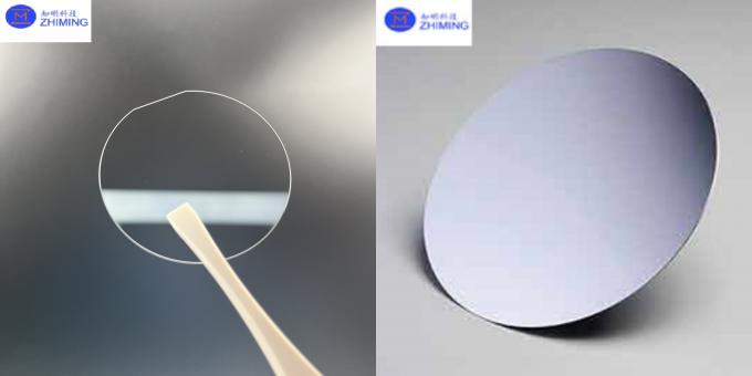
1. Кремниевые пластины: Основа полупроводниковой промышленности
Кремниевые пластины производятся из высокоочищенного монокристаллического кремния, выращенного, как правило, по методу Чохральского. После нарезки и полировки они служат базовой платформой для микрочипов и интегральных схем.
Основные характеристики материала
- Полупроводниковое поведение: Электропроводность можно точно контролировать с помощью легирования (P-тип или N-тип).
- Сильная промышленная зрелость: Десятилетия оптимизации процессов в производстве КМОП и МЭМС
- Масштабируемое производство: Доступны большие диаметры (до 300 мм в серийном производстве)
- Экономическая эффективность: Оптимизированная цепочка поставок и изобилие сырья
Основные сильные стороны
Главное преимущество кремния заключается в его управляемые электронные свойства, Это делает его стандартным выбором для логических схем, микросхем памяти и интеграции датчиков.
Типовые применения
- Микропроцессоры и микросхемы
- КМОП-датчики изображения
- МЭМС-устройства (акселерометры, гироскопы)
- Фотоэлектрические солнечные элементы
- Интегрированная фотоника (кремниевые фотонные платформы)
2. Сапфировые пластины: Оптическое и механическое превосходство
Сапфир - это монокристаллическая форма оксида алюминия (Al₂O₃). В отличие от кремния, он обладает электрической изоляцией, но механическими и оптическими свойствами в определенных условиях.
Основные характеристики материала
- Электрическая изоляция: Чрезвычайно высокое удельное сопротивление
- Широкое окно оптической передачи: От ультрафиолетового до ближнего инфракрасного
- Исключительная твердость: Твердость по шкале Мооса - 9 (уступает только алмазу)
- Химическая стабильность: Устойчивость к воздействию кислот, плазмы и жестких условий обработки
Почему сапфир выделяется
Сапфир не используется для традиционной проводки электрических цепей. Вместо этого он служит функциональной подложкой и защитным материалом, особенно там, где важны оптическая чистота и долговечность.
Типовые применения
- Подложки для светодиодов (особенно синих/ ультрафиолетовых светодиодов на основе GaN)
- Оптические окна в сенсорах и военных системах
- Смотровые окна для высокого давления и высоких температур
- Платформы для радиочастотных и микроволновых устройств
- Аэрокосмические и промышленные системы контроля
3. Кремний против сапфира: Сравнительная таблица инженерных решений
| Недвижимость | Кремниевая пластина | Сапфировая подложка |
|---|---|---|
| Электрическое поведение | Полупроводник | Электрический изолятор |
| Оптическая передача | Только инфракрасное излучение | Широкий диапазон от УФ до ИК |
| Твердость | Умеренный | Очень высокая (Мооса 9) |
| Теплопроводность | Высокий (хорошее рассеивание тепла) | Умеренный |
| Стоимость изготовления | Низкий | Высокий |
| Главная роль | Электроника и микросхемы | Оптика и защитные подложки |
4. Различия в оптических и фотонных характеристиках
Одно из самых важных отличий заключается в оптическом поведении.
Кремний поглощает видимый свет, что ограничивает его применение в оптических окнах или прозрачных устройствах. Однако он хорошо работает в системах на основе инфракрасного излучения, например в тепловизорах.
Сапфир, напротив, сохраняет высокую прозрачность в широком спектре, что делает его идеальным для использования:
- УФ-фотодетекторы
- Лазерные системы
- Оптические компоненты связи
- Системы визуализации высокого разрешения
Именно поэтому сапфир широко используется в оптоэлектронике, а не в логических схемах микроэлектроники.
5. Тепловая и механическая надежность в жестких условиях эксплуатации
В реальной технике материалы редко работают в идеальных условиях.
- Кремний эффективно работает в стандартной электронике, но может разрушаться под воздействием механических нагрузок.
- Сапфир обеспечивает превосходную устойчивость к царапинам и сохраняет структурную целостность при высоких температурах.
Например:
- В оборудовании для плазменной обработки сапфировые стекла противостоят коррозии гораздо лучше, чем большинство других материалов.
- В корпусах мощных светодиодов сапфир обеспечивает стабильность при постоянном термоциклировании.
6. Сложность производства и структура затрат
Кремний обладает развитой промышленной экосистемой:
- Крупномасштабный рост кристаллов
- Высокий выход пластин
- Развитая инфраструктура производства КМОП
Производство сапфиров более сложное:
- Медленный процесс роста кристаллов (методы Kyropoulos или EFG)
- Повышенная чувствительность к дефектам
- Более дорогая полировка и нарезка
В результате сапфировые подложки остаются значительно более дорогими в расчете на единицу площади.
Однако стоимость часто оправдывается более длительным сроком службы и высокой надежностью в сложных условиях эксплуатации.
7. Новые тенденции: Гибридные и передовые приложения
Современная полупроводниковая техника все чаще сочетает оба материала.
Примеры гибридного использования:
- GaN-на-сапфире для высокоэффективных светодиодов
- Микросхемы на основе кремния с сапфировыми оптическими окнами
- Радиочастотные устройства с использованием сапфира для снижения потерь сигнала
- Платформы фотонной интеграции, сочетающие кремниевую электронику и сапфировую оптику
Такой гибридный подход позволяет инженерам сбалансировать стоимость, производительность и долговечность.
8. Как выбрать правильные пластины
Решение зависит от требований к применению, а не от превосходства материала.
Выбирайте кремний, когда:
- Вы разрабатываете интегральные схемы или цифровые логические системы
- Стоимость и масштабируемость являются приоритетами
- Электрические характеристики - главная задача
Выбирайте Sapphire, когда:
- Требуется оптическая прозрачность
- Устройство работает в суровых условиях
- Механическая прочность и устойчивость к царапинам
- Применение ультрафиолетового излучения или высокочастотной оптики
Заключение
Кремний и сапфир представляют собой две принципиально разные инженерные философии.
Кремний оптимизирован для электрического интеллекта и масштабируемости, составляя основу современных вычислительных систем. Сапфир отличается оптической чистотой и устойчивостью к воздействию окружающей среды, что делает его незаменимым в оптоэлектронике и приложениях, работающих в экстремальных условиях.
Они не конкурируют напрямую, а дополняют друг друга в современных передовых архитектурах устройств.
Для высококачественных материалов подложек, используемых в промышленных и исследовательских приложениях, такие поставщики, как Stanford Advanced Materials (SAM), предлагают широкий спектр инженерных решений для кремниевых и сапфировых подложек.
ЧАСТО ЗАДАВАЕМЫЕ ВОПРОСЫ
Почему многие предпочитают использовать кремниевые пластины в стандартных электронных устройствах?
Кремниевые пластины обеспечивают очень контролируемое поведение полупроводников, что очень важно для схем. Они также хорошо переносят нагрев и производятся в больших объемах, что делает их экономически эффективными для стандартных устройств. Их длительное использование в электронной промышленности свидетельствует об их надежности.
Что делает сапфировые пластины пригодными для оптических применений?
Преимущество сапфировых пластин - прозрачность в диапазоне от ультрафиолетового до инфракрасного излучения. Их прочная, устойчивая к царапинам поверхность делает их идеальными для защитных стекол и высокоэффективных световых диодов. Они особенно предпочтительны для применения в суровых условиях, где долговечность имеет решающее значение.
Может ли в будущем измениться разрыв в стоимости между кремниевыми и сапфировыми пластинами?
Возможно, с развитием технологий производства разница в стоимости будет уменьшаться. Благодаря постоянным исследованиям и совершенствованию производственных процессов оба материала могут постепенно стать более доступными. Это позволит шире использовать сапфировые пластины в приложениях, требующих одновременно долговечности и высоких оптических характеристик.