
في مجال الإلكترونيات المتقدمة وتصنيع الإلكترونيات الضوئية، يحدد اختيار المواد بشكل مباشر أداء الجهاز وموثوقيته وهيكل التكلفة. ومن بين مواد الركيزة الأكثر انتشارًا رقائق السيليكون وركائز الياقوت.
على الرغم من استخدام كليهما في الصناعات المتعلقة بأشباه الموصلات، إلا أن أدوارهما مختلفة اختلافًا جوهريًا. يهيمن السيليكون على الدوائر المتكاملة التقليدية، بينما يتزايد استخدام الياقوت في الإلكترونيات الضوئية والأجهزة عالية التردد وتطبيقات البيئة القاسية.
تقدم هذه المقالة مقارنة تقنية أعمق من منظور هندسي عملي، مع التركيز على السلوك الكهربائي والخصائص البصرية والأداء الحراري وحالات الاستخدام الواقعية.
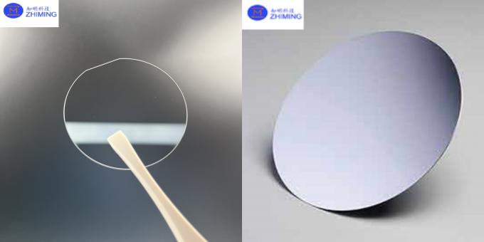
1. رقائق السيليكون: العمود الفقري لصناعة أشباه الموصلات
يتم إنتاج رقائق السيليكون من السيليكون أحادي البلورة عالي النقاء، وعادةً ما يتم زراعتها باستخدام طريقة Czochralski. وبعد تقطيعها وصقلها، تُستخدم كمنصة أساسية للرقائق الدقيقة والدوائر المتكاملة.
الخصائص المادية الرئيسية
- سلوك شبه موصل: يمكن التحكم في الموصلية الكهربائية بدقة من خلال التطعيم (النوع P أو النوع N)
- النضج الصناعي القوي: عقود من تحسين العمليات في تصنيع CMOS و MEMS
- التصنيع القابل للتطوير: متوفر بأقطار كبيرة (حتى 300 مم في الإنتاج الضخم)
- كفاءة التكلفة: سلسلة التوريد المحسنة للغاية ووفرة المواد الخام
نقاط القوة الرئيسية
تكمن أكبر ميزة للسيليكون في خصائص إلكترونية يمكن التحكم فيها, مما يجعلها الخيار الافتراضي للدوائر المنطقية ورقاقات الذاكرة وتكامل المستشعرات.
التطبيقات النموذجية
- المعالجات الدقيقة ورقاقات IC
- مستشعرات الصور CMOS
- أجهزة MEMS (أجهزة قياس التسارع والجيروسكوبات)
- الخلايا الشمسية الكهروضوئية
- الضوئيات المتكاملة (منصات ضوئيات السيليكون)
2. رقائق الياقوت: التميز البصري والميكانيكي
الياقوت هو شكل أحادي البلورة من أكسيد الألومنيوم (Al₂O₃). وعلى عكس السيليكون، فهو عازل كهربائيًا ولكنه متفوق ميكانيكيًا وبصريًا في بيئات معينة.
الخصائص المادية الرئيسية
- العزل الكهربائي: مقاومة عالية للغاية
- نافذة إرسال بصري عريضة: الأشعة فوق البنفسجية إلى الأشعة تحت الحمراء القريبة
- صلابة استثنائية: صلابة موس 9 (تأتي في المرتبة الثانية بعد الماس)
- الثبات الكيميائي: مقاومة للأحماض والبلازما وبيئات المعالجة القاسية
لماذا يبرز الياقوت الأزرق
لا يُستخدم الياقوت لتوصيل الدوائر الكهربائية التقليدية. وبدلاً من ذلك، فإنه يُستخدم كركيزة وظيفية ومادة واقية، خاصةً عندما يكون الوضوح البصري والمتانة أمرًا بالغ الأهمية.
التطبيقات النموذجية
- ركائز الصمام الثنائي الباعث للضوء (خاصةً مصابيح LED الزرقاء/الأشعة فوق البنفسجية القائمة على الغاليوم)
- نوافذ بصرية في أجهزة الاستشعار والأنظمة العسكرية
- منافذ عرض الضغط العالي والحرارة العالية
- منصات أجهزة الترددات اللاسلكية والموجات الدقيقة
- أنظمة فحص الفضاء الجوي والصناعي
3. السيليكون مقابل الياقوت: جدول المقارنة الهندسية
| الممتلكات | رقاقة السيليكون | ركيزة من الياقوت الأزرق |
|---|---|---|
| السلوك الكهربائي | أشباه الموصلات | عازل كهربائي |
| الإرسال الضوئي | الأشعة تحت الحمراء فقط | نطاق عريض من الأشعة فوق البنفسجية إلى الأشعة تحت الحمراء |
| الصلابة | معتدل | عالية للغاية (موس 9) |
| التوصيل الحراري | عالية (تبديد جيد للحرارة) | معتدل |
| تكلفة التصنيع | منخفضة | عالية |
| الدور الرئيسي | الإلكترونيات والدوائر المتكاملة | البصريات والركائز الواقية |
4. الاختلافات في الأداء البصري والضوئي
يكمن أحد أكثر الفروق أهمية في السلوك البصري.
يمتص السيليكون الضوء المرئي، مما يحد من استخدامه في النوافذ البصرية أو الأجهزة الشفافة. ومع ذلك، فإنه يعمل بشكل جيد في الأنظمة القائمة على الأشعة تحت الحمراء مثل التصوير الحراري.
من ناحية أخرى، يحافظ الياقوت الأزرق على شفافية عالية عبر طيف واسع، مما يجعله مثاليًا لـ
- أجهزة الكشف الضوئي بالأشعة فوق البنفسجية
- أنظمة الليزر
- مكونات الاتصالات البصرية
- أنظمة تصوير عالية الدقة
وهذا هو سبب استخدام الياقوت على نطاق واسع في الإلكترونيات الضوئية بدلاً من الدوائر المنطقية للإلكترونيات الدقيقة.
5. الموثوقية الحرارية والميكانيكية في البيئات القاسية
في هندسة العالم الحقيقي، نادرًا ما تعمل المواد في ظروف مثالية.
- يعمل السيليكون بكفاءة في الإلكترونيات القياسية ولكن يمكن أن يتحلل تحت الضغط الميكانيكي.
- يوفر الياقوت مقاومة فائقة للخدش ويحافظ على السلامة الهيكلية في درجات الحرارة العالية.
على سبيل المثال:
- في معدات معالجة البلازما، تقاوم نوافذ الياقوت التآكل بشكل أفضل بكثير من معظم المواد.
- في تغليف مصابيح LED عالية الطاقة، يضمن الياقوت ثباتًا في ظل التدوير الحراري المستمر.
6. تعقيد التصنيع وهيكل التكلفة
يستفيد السيليكون من النظام البيئي الصناعي الناضج:
- نمو البلورات على نطاق واسع
- إنتاجية عالية للرقاقة
- بنية تحتية راسخة لتصنيع CMOS
يُعد إنتاج الياقوت أكثر تعقيداً:
- عملية النمو البلوري البطيء (طرق كيروبولوس أو EFG)
- حساسية أعلى للعيوب
- تلميع وتقطيع أكثر تكلفة
ونتيجة لذلك، تظل ركائز الياقوت أغلى بكثير لكل وحدة مساحة.
ومع ذلك، غالبًا ما يتم تبرير التكلفة بعمر افتراضي أطول وموثوقية أعلى في التطبيقات الصعبة.
7. الاتجاهات الناشئة: التطبيقات الهجينة والمتقدمة
تجمع هندسة أشباه الموصلات الحديثة بين المادتين بشكل متزايد.
أمثلة على الاستخدام المختلط:
- GaN على الياقوت الأزرق لمصابيح LED عالية الكفاءة
- دارات قائمة على السيليكون مع نوافذ بصرية من الياقوت الأزرق
- أجهزة التردد اللاسلكي باستخدام الياقوت لتقليل فقدان الإشارة
- منصات التكامل الضوئي التي تجمع بين إلكترونيات السيليكون والبصريات الياقوتية
يتيح هذا النهج الهجين للمهندسين تحقيق التوازن بين التكلفة والأداء والمتانة.
8. كيفية اختيار الرقائق المناسبة
يعتمد القرار على متطلبات التطبيق وليس على التفوق المادي.
اختر السيليكون عندما:
- كنت تقوم بتصميم دوائر متكاملة أو أنظمة منطقية رقمية
- التكلفة وقابلية التوسع من الأولويات
- الأداء الكهربائي هو الشاغل الرئيسي
اختر الياقوت عندما:
- الشفافية البصرية مطلوبة
- يعمل الجهاز في البيئات القاسية
- المتانة الميكانيكية ومقاومة الخدوش أمران مهمان
- تطبيقات الأشعة فوق البنفسجية أو التطبيقات البصرية عالية التردد
الخاتمة
يمثّل السيليكون والياقوت فلسفتين هندسيتين مختلفتين اختلافاً جوهرياً.
تم تحسين السيليكون للذكاء الكهربائي وقابلية التوسع، مما يشكل العمود الفقري للحوسبة الحديثة. صُمم الياقوت من أجل الوضوح البصري والمرونة البيئية، مما يجعله لا غنى عنه في الإلكترونيات الضوئية والتطبيقات ذات الظروف القاسية.
فبدلاً من التنافس المباشر، فإنهما يكملان بعضهما البعض في بنيات الأجهزة المتقدمة اليوم.
بالنسبة لمواد الركيزة عالية الجودة المستخدمة في التطبيقات الصناعية والبحثية، يوفر الموردون مثل ستانفورد أدفانسد أدفانسد ماتيريالز (SAM) مجموعة واسعة من حلول الرقائق المصممة هندسيًا لكل من أنظمة السيليكون والياقوت.
الأسئلة الشائعة
لماذا يختار الكثيرون رقائق السيليكون في الأجهزة الإلكترونية القياسية؟
توفر رقائق السيليكون سلوك أشباه الموصلات المتحكم فيه للغاية وهو أمر ضروري للدوائر. كما أنها تتعامل مع الحرارة بشكل جيد ويتم إنتاجها بكميات كبيرة، مما يجعلها فعالة من حيث التكلفة للأجهزة القياسية. ويشهد استخدامها لفترة طويلة في قطاع الإلكترونيات على موثوقيتها.
ما الذي يجعل رقائق الياقوت مناسبة للتطبيقات البصرية؟
تتميز رقائق الياقوت بميزة الشفافية الواضحة عبر نطاق الأشعة فوق البنفسجية إلى الأشعة تحت الحمراء. كما أن سطحها القوي المقاوم للخدش يجعلها مثالية للنوافذ الواقية والثنائيات الضوئية عالية الأداء. وهي مفضلة بشكل خاص في تطبيقات البيئة القاسية حيث تكون المتانة أمرًا بالغ الأهمية.
هل يمكن أن تتغير الفجوة في التكلفة بين رقائق السيليكون والياقوت في المستقبل؟
ومن الممكن أن يقل فرق التكلفة مع تطور تقنيات الإنتاج. ومع الأبحاث الجارية وعمليات التصنيع المحسّنة، قد تصبح كلتا المادتين تدريجيًا أقل تكلفة. وقد يسمح ذلك باستخدام رقاقات الياقوت على نطاق أوسع في التطبيقات التي تتطلب المتانة والأداء البصري العالي.